TLV9001 Low-Power, RRIO, 1-MHz Operational Amplifier for Cost-Sensitive Systems
The TLV9001 includes a single operational amplifier (op-amps) with rail-to-rail input and output swing capabilities. These op-amps provide a cost-effective solution for space-constrained applications such as smoke detectors, wearable electronics, and small appliances where low-voltage operation and high capacitive-load drive are required.
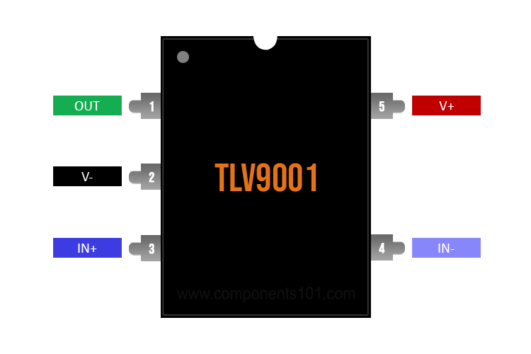
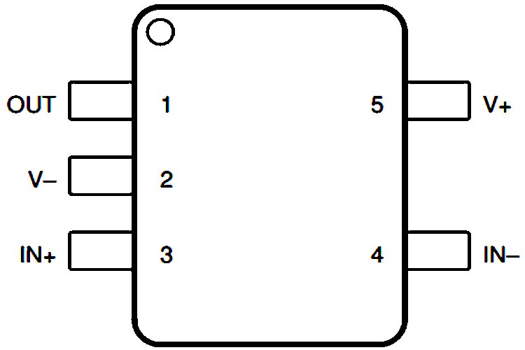
TLV9001 Op-Amp Pinout Configuration
|
Pin Number |
Pin Name |
Description |
|
1 |
Out |
Output of Op-Amp |
|
2 |
V- |
Ground or Negative(Dual Polarity Supply) |
|
3 |
Inverting Input |
Inverting Input of Op-Amp |
|
4 |
Non-Inverting Input |
Non-Inverting Input of Op-Amp |
|
5 |
V+ |
Supply Voltage |
Features & Specifications
- Superior Sound Quality
- Ultra-Low Distortion: 0.0008%
- Scalable CMOS amplifier for low-cost applications
- Rail-to-rail input and output
- Low input offset voltage: ±0.4 mV
- Unity-gain bandwidth: 1 MHz
- Low broadband noise: 27 nV/√ Hz
- Low input bias current: 5 pA
- Low quiescent current: 60 µA/Ch
- Unity-gain stable
- Internal RFI and EMI filter
- Operational at supply voltages as low as 1.8 V
- Easier to stabilize with higher capacitive load due to resistive open-loop output impedance
- Extended temperature range: –40°C to 125°C
Note: Complete technical details can be found in the TLV9001 datasheet given at the end of this page.
TLV9001 Equivalent Op-Amp
TL074, TL072, LMH9200, TLV9031, TLV9041
Where to use TLV9001 Op-Amp
The TLV9001 is a Single Package Operational Amplifier, meaning it has a single Op-Amps inside it and can be used in many different applications.
The main distinguishing feature of the TLV9001 Op-Amp is that they are ultra-low distortion, low-noise operational amplifiers fully specified for audio applications. a cost-effective solution for space-constrained applications such as smoke detectors, wearable electronics, and small appliances where low-voltage operation and high capacitive-load drive are required. The capacitive-load drive of the TLV9001 is 500 pF, and the resistive open-loop output impedance makes stabilization easier with much higher capacitive loads. These op-amps are designed specifically for low-voltage operation (1.8 V to 5.5 V) with performance specifications similar to the TLV600x devices.
The robust design of the TLV9001 family simplifies the circuit design. The op-amps feature unity-gain stability, an integrated RFI and EMI rejection filter, and no-phase reversal in overdrive conditions. The TLV900x devices include a shutdown mode (TLV9001S, TLV9002S, and TLV9004S) that allows the amplifiers to switch off into standby mode with typical current consumption of less than 1 µA. Micro-size packages, such as SOT-553 and WSON, are offered for all channel variants (single, dual, and quad), along with industry-standard packages such as SOIC, MSOP, SOT-23, and TSSOP packages.
Special Features of TLV9001 IC
The TLV9001 is a low-power, rail-to-rail input, and output op-amps. These devices operate from 1.8 V to 5.5 V, and are unity-gain stable, and are designed for a wide range of general-purpose applications. The input common-mode voltage range includes both rails and allows the TLV9001 devices to be used in any single-supply application. Rail-to-rail input and output swing significantly increases dynamic range, especially in low-supply applications, and makes them suitable for driving sampling analog-to-digital converters (ADCs).
Rail-to-Rail Input:
The input common-mode voltage range extends 100 mV beyond the supply rails for the full supply voltage range of 1.8 V to 5.5 V. This performance is achieved with a complementary input stage: an N-channel input differential pair in parallel with a P-channel differential pair as shown in the image below. The N-channel pair is active for input voltages close to the positive rail, typically (V+) – 1.4 V to 100 mV above the positive supply, whereas the P-channel pair is active for inputs from 100 mV below the negative supply to approximately (V+) – 1.4 V.
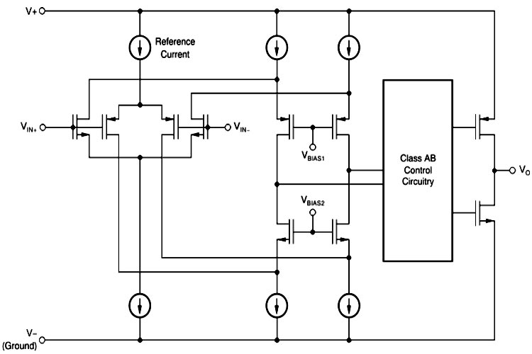
Rail-to-Rail Output:
Designed as a low-power, low-voltage operational amplifier, the TLV9001 is a robust output drive capability. A class-AB output stage with common-source transistors achieves full rail-to-rail output swing capability. For resistive loads of 10 kΩ, the output swings to within 20 mV of either supply rail, regardless of the applied power-supply voltage. Different load conditions change the ability of the amplifier to swing close to the rails.
EMI Rejection:
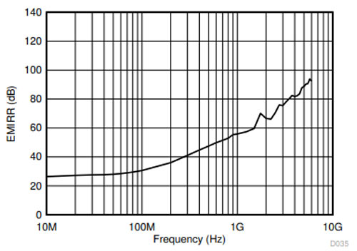
The TLV9001 uses integrated electromagnetic interference (EMI) filtering to reduce the effects of EMI from sources such as wireless communications and densely-populated boards with a mix of the analog signal chain and digital components. EMI immunity can be improved with circuit design techniques; the TLV900x benefits from these design improvements.
Overload Recovery:
Overload recovery is defined as the time required for the operational amplifier output to recover from a saturated state to a linear state. The output devices of the operational amplifier enter a saturation region when the output voltage exceeds the rated operating voltage, because of the high input voltage or the high gain. After the device enters the saturation region, the charge carriers in the output devices require time to return to the linear state. After the charge carriers return to the linear state, the device begins to slew at the specified slew rate. Therefore, the propagation delay (in case of an overload condition) is the sum of the overload recovery time and the slew time. The overload recovery time for the TLV9001 is approximately 850 ns.
How to use TLV9001 Op-Amp
In the circuit shown below, we have configured the TLV9001 IC in a low side current sensing application,
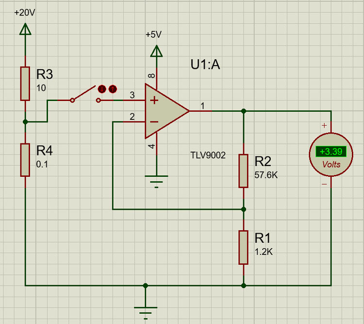
In the above, the Op-amp is configured as a low-side current sensor, The transfer function of the circuit is in. The load current (ILOAD) produces a voltage drop across the shunt resistor (RSHUNT). The load current is set from 0 A to 1 A. To keep the shunt voltage below 100 mV at maximum load current, the largest shunt resistor is shown the gain of the circuit can be found by implementing a gain formula.
Applications
- Sensor signal conditioning
- Power modules
- Active filters
- Low-side current sensing
- Smoke detectors
- Motion detectors
- Wearable devices
- Large and small appliances
- EPOS
- Barcode scanners
- Personal electronics
- HVAC: heating, ventilating, and air conditioning
- Motor control: AC induction
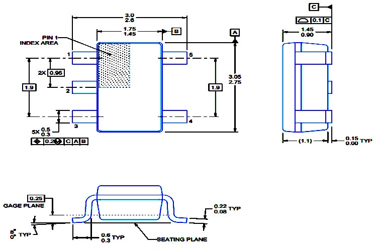
2D Model and Dimensions
If you are designing a PCB or Perf board with this component then the following picture from the Datasheet will be useful to know its package type and dimensions.