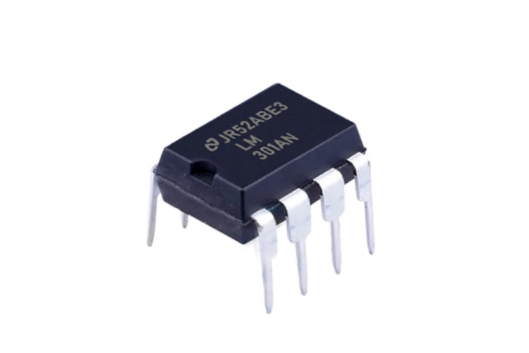
LM301 Op-Amp IC
The LMx01 family of op-amps was designed by the legendary Bob Widlar in the late 1960s, and still remains one of the best op-amps in its class. One interesting feature of this op-amp is that it is uncompensated, meaning that the compensation capacitor that is usually present on-die is broken out into two pins, so the user can compensate the op-amp according to their needs, which will be covered later in this article.
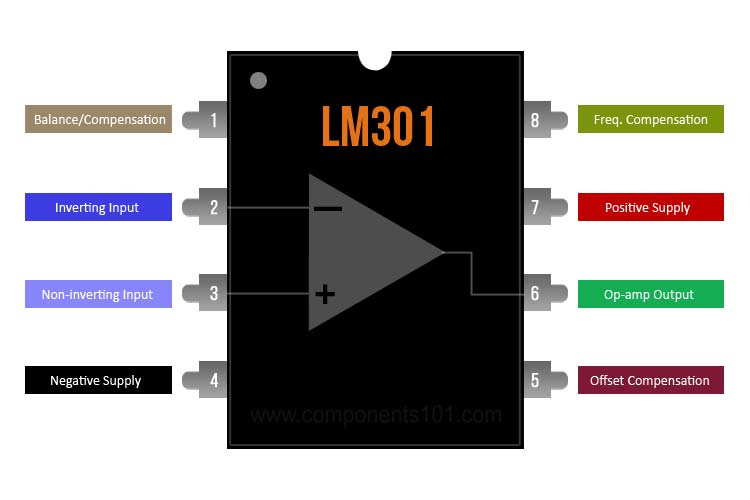
LM301 Pinout Configuration
|
Pin Number |
Pin Name |
Description |
|
1 |
BAL/COMP |
Shared pin for frequency and offset compensation |
|
2 |
- INPUT |
Inverting input |
|
3 |
+ INPUT |
Non-inverting input |
|
4 |
V- |
Negative supply pin |
|
5 |
BAL |
Offset compensation pin |
|
6 |
OUTPUT |
Op-amp output |
|
7 |
V+ |
Positive supply pin |
|
8 |
COMP |
Frequency compensation pin |
Features and Specifications
- 3mV offset voltage, 100nA bias, and 20nA offset current
- Slew rate of 10V/us (as summing amplifier)
- Externally compensated
Note: Complete technical details can be found in the LM301a datasheet given at the end of this page.
LM301 Equivalents
LM318
Other Op-Amps
How To Use LM301?
The LMx01 family consists of three parts, LM101, LM201, and LM301, with the only difference being the specified temperature range – the LM101 for military (-55˚C to +125˚C), LM201 for industrial (-25˚C to +85˚C), and LM301 (0˚C to +75˚C) for commercial temperature ranges.
Most op-amps on the market are internally compensated, which saves some headache, but there are situations where external (or even switchable) compensation might be necessary. In the case of the LM301, the compensation is provided by connecting a suitable network between pins 1 and 8, as shown in the figure below. The value of the compensation capacitor depends upon the application.
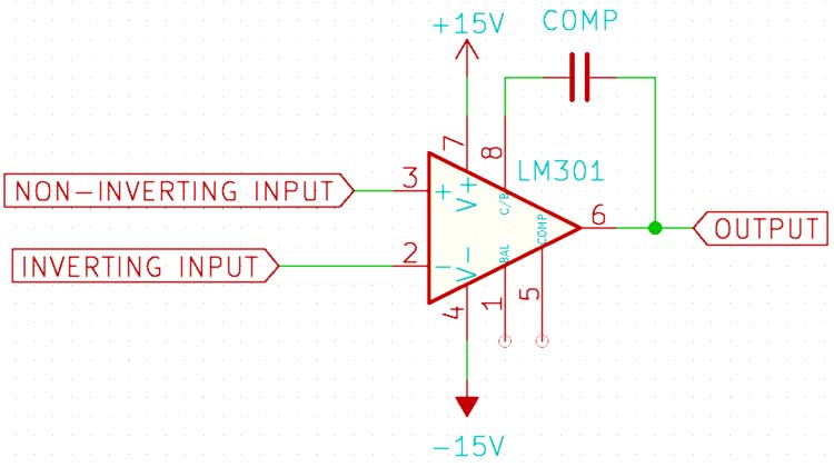
Leaving these pins unconnected is not recommended, as it can lead to unspecified behavior and oscillations, and stray capacitance. The datasheet also shows more complicated compensation methods like two-pole and feedforward compensation.
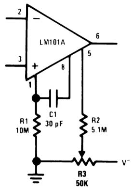
Another thing to note is that the slew rate depends upon the compensation. The datasheet specifies a slew rate of 10V/us when connected as an inverting (summing) amplifier. Offset balance pins are also provided, which can be used to null the offset voltage. An example circuit is shown in the figure below.
Applications
- Long interval integrators/timers
- Sample and hold circuits
- Low-frequency waveform generators
2D Model and Dimensions
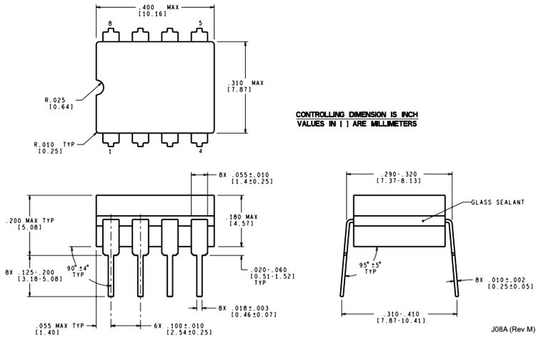
If you are designing a PCB or Perf board with this component then the following picture from the Datasheet will be useful to know its package type and dimensions.
