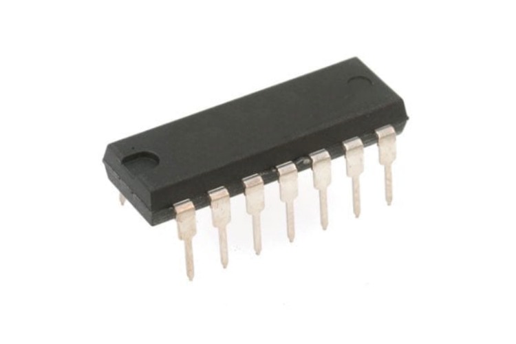
SN74LS74AN Dual D Flip-Flop IC
The SN74LS74AN is a dual D flip-flop manufactured by Texas Instruments containing two independent positive-edge triggered D flip-flops with set and reset inputs. The SN74 family is characterized for operation from 0 °C to 70 °C.
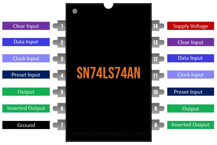
SN74LS74AN Pinout Configuration
|
Pin Number |
Pin Name |
Description |
|
14 |
VCC |
Supply voltage, 5V nominal |
|
1, 13 |
|
Clear input, equivalent to reset |
|
2, 12 |
D |
Data input |
|
3, 11 |
CLK |
Clock input, rising edge triggered |
|
4, 10 |
|
Preset input, equivalent to set |
|
5, 9 |
Q |
Output |
|
6, 8 |
|
Inverted output |
|
7 |
GND |
IC ground reference |
Features and Specifications
- Dual D flip-flops in the same package
- Positive edge-triggered
- Preset and Clear inputs
Note: Complete technical details can be found in the SN74LS74AN datasheet linked at the end of this page.
SN74LS74AN Equivalents
74HC74, 74HCT74
Other D Flip-Flops
How To Use SN74LS74AN?
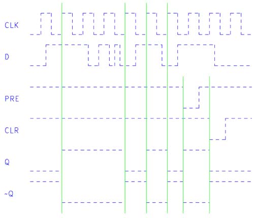
The SN74LS74AN is a dual D-type positive edge-triggered flip-flop with set and clear inputs.
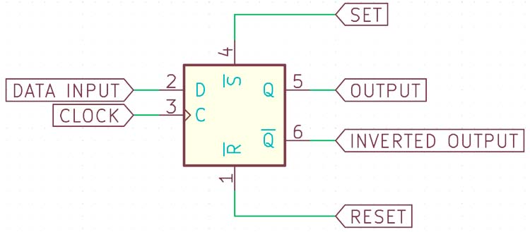
A flip-flop is a basic ‘memory’ circuit – the output remembers the previous input state unless the power to the IC is turned off. Data is fed into the D pin (D for data), and when the chip registers a rising edge on the CLK (clock) pin, the data is transferred to the Q and  pins. After this, any input on the D pin does not get transferred to the output pins unless there is once again a rising edge on the CLK pin.
The CLK pin is usually fed with a periodic clock signal, and this can be used to synchronize external inputs to a clocked synchronous circuit.
The SN74LS74AN also comes with  and
and  pins, which is the equivalent of set and reset pins on a regular flip-flop. On this chip, these two inputs override the D and CLK pins – regardless of their state, setting low turns Q high and low, and setting low turns Q low and high. If these pins are not used, they can be tied to VCC.
The ‘LS’ in the part number means low-power Schottky, meaning that the transistors that make up the IC are NPN transistors with a base-collector Schottky diode that prevents saturation and speeds up the transistor. This also means that the input logic thresholds are 0.8V for low and 2V for high respectively, which might not be compatible with other logic ICs, care should be taken while interfacing ICs between logic families.
Applications
- Data storage
- Data synchronization
- Quadrature generator
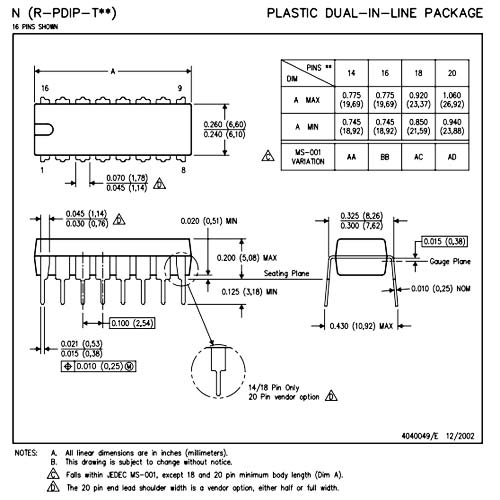
2D Model and Dimensions
If you are designing a PCB or Perf board with this component then the following picture from the Datasheet will be useful to know its package type and dimensions.