MJE3055T - NPN Silicon Power Transistor
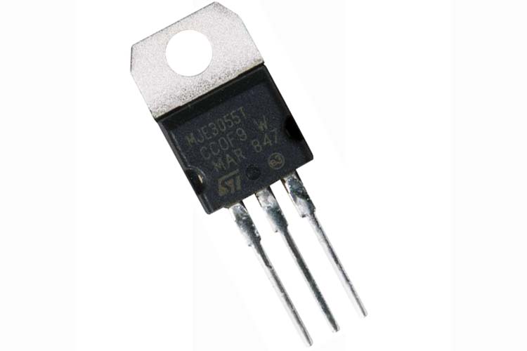
MJE3055T is a general-purpose NPN power transistor manufactured with the epitaxial base process and mounted in a hermetically sealed metal case. This device is designed for general purpose switching and amplifier applications.
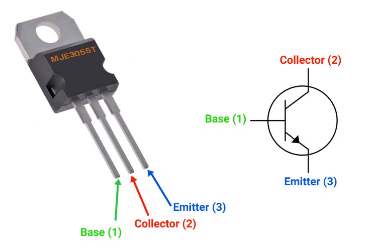
MJE3055T Pinout Configuration
Like any other transistor, MJE3055T has three pins namely EMITTER, BASE, and COLLECTOR. The pin configuration of MJE3055T is given below.
|
Pin Number |
Pin Name |
Description |
|
1 |
Base |
Controls the biasing of the transistor |
|
2 |
Collector |
Electrons Emitted from Emitter Collected by the Collector |
|
3 |
Emitter |
Electrons emitted from the emitter into the first PN junction |
Features & Specifications
- Bi-Polar NPN Power Transistor
- DC Current Gain (hFE) is 100 maximum
- Continuous Collector current (IC) is 10A
- Emitter Base Voltage (VBE) is 5V
- Base Current (IB) is 6A maximum
- Available in TO-220 Package
- Maximum Collector-Base Voltage |Vcb|: 70 V
- Collector Dissipation: 75 W
- Transition Frequency: 2 MHz
- Operating Junction Temperature Max (Tj): 175 °C
- Noise Figure: 2-10 dB
- Operating and Storage Junction Temperature Range -55 to +150 °C
- Collector Capacitance 8.5 pF
- Pb−free packages are available
Note: Complete Technical Details can be found in the MJE3055T datasheet given at the end of this page.
MJE3055T Transistor Equivalents
2N6673, 2N3055, TIP122, 2N6675
How to use MJE3055T Transistor in a Circuit
The MJE3055T transistor is a very versatile transistor that can be used in many different applications. It is used in high-power applications where we need to control high power loads. The frequency range of this transistor is quite limited which is why it is mostly used in amplifiers, but in some cases, it can be configured as a preamplifier for a power amplifier stage.
As we have mentioned earlier the MJE3055T is an NPN transistor and can be used in many different applications, for that reason we have set the transistor in a common emitter configuration, and we are driving a high-power motor as load. Under initial circumstances, the button will be in open circuit condition and no current will flow through the base. With no base current, the transistor acts as an open circuit and the entire supply voltage V1 will not appear across it.
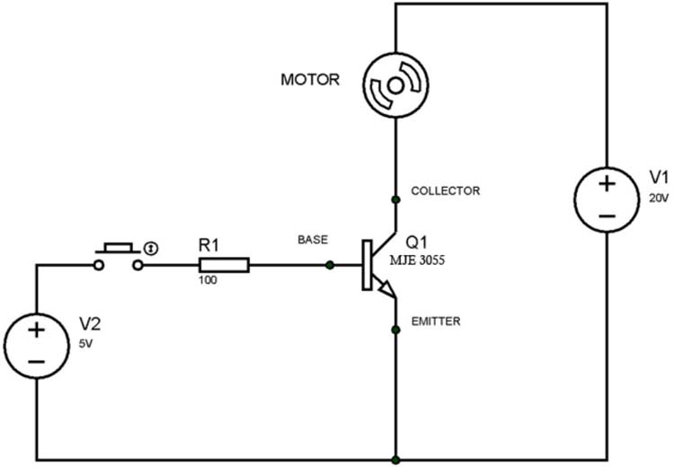
When the button is pressed the voltage V2 forms a closed loop with base-emitter of transistor as can be seen in the circuit diagram shown above. With a complete circuit, current flows through the base to the emitter, and the transistor turns on, after a certain time when the button is released, the base current becomes zero and the transistor shuts down. With the transistor going to a high resistance state in OFF mode, the collector current also becomes zero bringing the motor to stop rotating.
Applications
- Power switching circuits
- Amplifier circuits
- PWM applications
- Regulator circuits
- Switch-mode power supply
- Signal Amplifiers
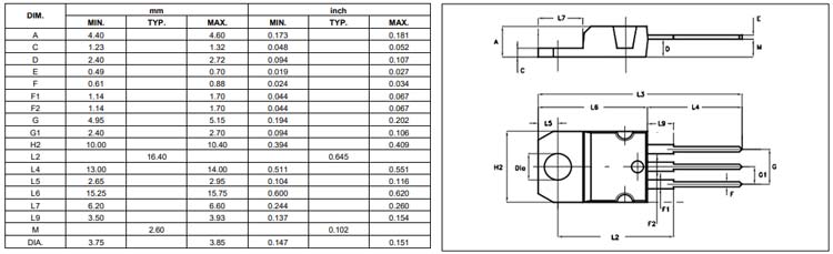
2D Model and Dimensions
If you are designing a PCB or Perf board with this component, then the following picture from the Datasheet will be useful to know its package type and dimensions.