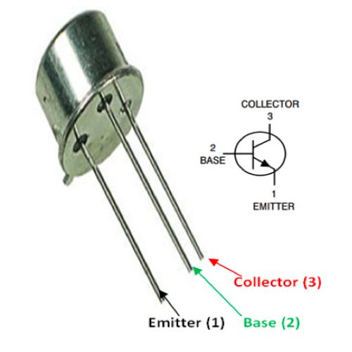
BC107 NPN Transistor
The BC107 is a small single NPN Transistor available in TO-18 metal can package. These transistors are age old and have been used in low noise and low signal designs. Today a lot new transistors have come as replacement for BC107, but still the transistor can be found in market for its legacy.
Pin Configuration
|
Pin Number |
Pin Name |
Description |
|
1 |
Emitter |
Current Drains out through emitter, normally connected to ground |
|
2 |
Base |
Controls the biasing of transistor, Used to turn ON or OFF the transistor |
|
3 |
Collector |
Current flows in through collector, normally connected to load |
Features
- Small Signal NPN Transistor
- Current Gain (hFE): 450 (maximum)
- Continuous Collector current (IC) is 100mA
- Collector-Emitter voltage (VCEO) is 45V
- Collector-Base voltage (VCB0) is 50V
- Emitter Base Voltage (VBE0) is 6V
- Available in To-18 Metal can Package
Note: Complete Technical Details can be found at the BC107 datasheet given at the end of this page.
Alternative NPN Transistors
BC107 Equivalent
PNP Complementary for BC107
Where to use BC107 Transistor
The BC107 is a low signal NPN which is known for its low noise operations making it famously used in signal processing circuits and television receivers. The transistor is still available in market due to its legacy but you will find better modern transistors as replacement for BC107.
Brief Description on BC107 Transistor
BC107 is a NPN transistor hence the collector and emitter will be left open (Reverse biased) when the base pin is held at ground and will be closed (Forward biased) when a signal is provided to base pin. BC107 has a gain value hfe of 50; this value determines the amplification capacity of the transistor. The maximum amount of current that could flow through the Collector pin is 100mA, hence we cannot connect loads that consume more than 100mA using this transistor.
When this transistor is fully biased then it can allow a maximum of 100mA to flow across the collector and emitter. This stage is called Saturation Region. When base current is removed the transistor becomes fully off, this stage is called as the Cut-off Region.
Applications
- Driver Modules like Relay Driver, LED driver etc..
- Amplifier modules like Audio amplifiers, signal Amplifier etc..
- Darlington pair
2D model of the component
If you are designing a PCD or Perf board with this component then the following picture from the Datasheet will be useful to know its package type and dimensions.


.jpg)


