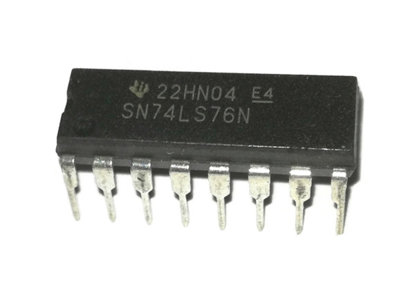
74LS76 Dual JK Flip-Flop
The 74LS76 offers individual J, K, Clock Pulse, Direct Set, and Direct Clear inputs. These dual flip-flops are designed so that when the clock goes HIGH, the inputs are enabled and data will be accepted.
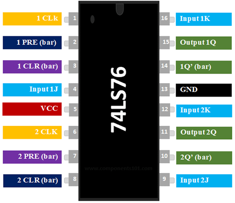
Pin Description of 74LS76:
|
Pin Number |
Pin Name |
Description |
|
5 |
Vcc |
Powers the IC typically with 5V |
|
13 |
Ground |
Connected to the ground of the system |
|
JK Flip Flop – 1 / JK Flip Flop - 2 |
||
|
1,6 |
Clock-1/ Clock-2 |
These pins must be provided with clock pulse for the flip flop |
|
2,7 |
Preset-1 / Preset-2 |
Preset input pin drives Flip Flop to a set state. |
|
16, 12 |
1K/ 2K |
Input pin of the Flip Flop |
|
4,9 |
1J / 2J |
Another Input pin of the Flip Flop |
|
14, 10 |
1Q(bar) / 2Q (bar) |
Inverted output pin of Flip Flop |
|
15,11 |
1Q / 2Q |
Output Pin of the Flip Flop |
|
3,8 |
1 CLR (bar)/ 2 CLR (bar) |
Clear input pin drives Flip Flop to a reset state. |
Features of 74LS76:
- Dual JK Flip Flop Package IC
- Operating Voltage: 2V to 6V
- Minimum High Level Input Voltage: 2 V
- Maximum Low Level Input Voltage: 0.8 V
- Minimum High Level Output Voltage: 3.5 V
- Maximum Low Level Output Voltage: 0.25V
- Operating Temperature -55 to -125°C
- Available in 14-pin PDIP, GDIP, PDSO packages
Note: Complete Technical Details can be found at the 74LS76 datasheet give at the end of this page.
Equivalent for 74LS76: 74LS73, MC74HC73A, SN7476
Alternatives JK Flip-Flop: 74LS107, 4027B
Where to use 74LS76 JK Flip-Flop:
The 74LS76 is a dual in-line JK flip flop IC. Meaning it has two JK flip flops inside it and each can be used individually based on our application. The JK flip flops are considered to be the most efficient flip-flop and can be used for certain applications on its own. The flip-flops are also called latching devices meaning it can remember one single bit of data and latch the output based on it, due to this property they are commonly used as shift registers, control registers, storage registers or where ever a small memory is required. More than one Flip Flop can be used in series to act as an EEPROM for holding a small amount of data. The JK flip flop is considered to be more suitable for practical application because of its truth table that is the output of the flip flop will be stable for all types of inputs.
So if you are looking for an IC for latching purpose or to act as a small programmable memory for you project then this IC might be the right choice for you.
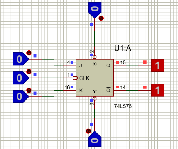
How to use 74LS76:
As told earlier we have two JK flip flops in this IC, the IC is powered by +5V typically. The minimum and maximum input and output voltage for the input (J, K) pins and the output (Q, Q bar) pins are discussed in the specifications above. Working of J-K flip flop is shown in the GIF below
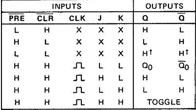
The preset and clear are asynchronous active-low inputs. When preset and clear are set low they override the clock and J-K inputs forcing the output to the steady-state levels as shown in the truth table below.
Applications of 74LS76
- Shift Registers
- Memory/Control Registers
- EEPROM circuits
- Latching devices
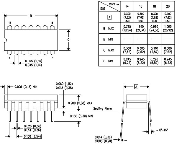
2D Model of 74LS76
Dimensions for 74LS76 IC is given below. These dimensions are for GDIP package. If you are using different package IC please refer to 74LS76 datasheet.