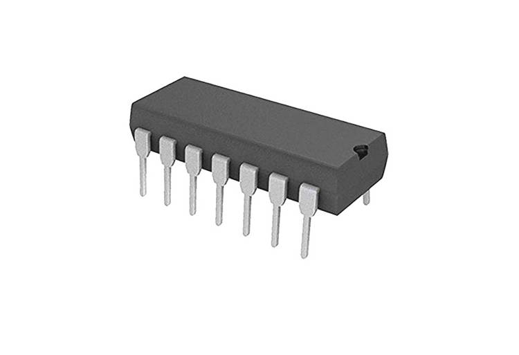
74HCT20 Dual 4-Input NAND Gate
The CD74HCT20M is a high speed CMOS Logic dual 4-input NAND Gate. The logic gates utilize silicon gate CMOS technology to achieve operating speeds similar to LSTTL gates with the low power consumption of standard CMOS integrated circuits. It is commonly used in buffer circuits, logic inverter circuits etc.
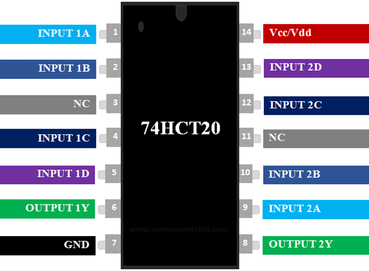
Pin Description of 74HCT20:
|
Pin Number |
Pin Name |
Description |
|
6 |
NAND Gate Output pin (1) |
Output pin of NAND Gate - 1 |
|
1,2,4,5 |
NAND Gate Input pin (1) |
Four Input pins of NAND Gate -1 |
|
7 |
Ground |
Connect to the ground of the circuit. |
|
9,10,12,13 |
NAND Gate Input pin (2) |
Four Input pins of NAND Gate -2 |
|
8 |
NAND Gate Output pin (2) |
Output pin of NAND Gate - 2 |
|
14 |
Vcc (Vdd) |
Used to power the IC. Typically +5V is used |
Features of 74HCT20:
- Four Input OR Gate – Dual Package
- Typical Operating Voltage: 5V
- Power Dissipation: 500mW
- Propagation Delay @5V: 8ns (maximum)
- Available in 14-pin PDIP, GDIP, PDSO packages
Note: Complete Technical Details can be found at the 74HCT20 datasheet give at the end of this page.
Equivalent for 74HCT20: CD4012, 74S140, 74HC20
Other Logic Gates: 74LS00, 74LS08, 74LS02, 74LS04, 74HCT04
How to use 74HCT20:
The 74HCT20 is a dual 4-Input NAND gate IC from the Logic Gate family ICs. It can take in four logic inputs and provide an output based on the NAND Gate truth table. Inputs include clamp diodes. This enables the use of current limiting resistors to interface inputs to voltages in excess of VCC. NAND gate is commonly used in buffer circuits and logic inverter circuits for digital communication. Both 74HCT20 and 74HC20 are very similar to each other by pinout and features.
4-Input NAND Gate Truth Table:
| Input A | Input B | Input C | Input D | Output Y |
| 0 | 0 | 0 | 0 | 1 |
| 0 | 0 | 0 | 1 | 1 |
| 0 | 0 | 1 | 0 | 1 |
| 0 | 0 | 1 | 1 | 1 |
| 0 | 1 | 0 | 0 | 1 |
| 0 | 1 | 0 | 1 | 1 |
| 0 | 1 | 1 | 0 | 1 |
| 0 | 1 | 1 | 1 | 1 |
| 1 | 0 | 0 | 0 | 1 |
| 1 | 0 | 0 | 1 | 1 |
| 1 | 0 | 1 | 0 | 1 |
| 1 | 0 | 1 | 1 | 1 |
| 1 | 1 | 0 | 0 | 1 |
| 1 | 1 | 0 | 1 | 1 |
| 1 | 1 | 1 | 0 | 1 |
| 1 | 1 | 1 | 1 | 0 |
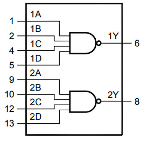
To use the 74HCT20 IC, just power it using the Vcc and ground lines. The typical operating voltage of the IC is +5V. The output voltage of the IC on the pin Y will be equal to the operating voltage of the IC. As per the NAND Gate 4 input truth table shown above, when either one or both the input of the Gate is high the output will be high. Internal circuit diagram of 74HCT20 is given below:
Applications of NAND Gate:
- Logic Buffer circuit
- Basic Logic Circuits
- Encoders and Decoders
- Multiplexers and De-multiplexers
- Oscillator circuits
- Networking and Digital Systems
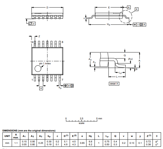
2D-Model of 74HCT20: