What is an LDO Regulator and Important Parameters to Select an LDO

Low dropout regulator (LDO) is a simple and cost-effective voltage regulator to get a regulated output voltage from a higher input voltage. The special feature of an LDO is its ability to have a very low voltage drop across it when providing a regulated output voltage. This allows the LDO to be used in power critical battery applications where the battery voltage (input voltage) is close to the required regulated output voltage.
LDO takes in a variable input voltage and provides a continuously controlled, steady, low-noise DC output voltage. LDO is a linear voltage regulator that has a small voltage drop between the input and the output, and it works well even when the output voltage is very close to the input voltage unlike the linear voltage regulator that requires a large voltage drop between the input and the output to work properly. LDO has no switching noise (as no switching takes place), and has a smaller device size as compared to linear voltage regulators.
There are two main functions of an LDO; the first function is to regulate the input supply voltage to the voltage required by the load and second function is to supply a very low-noise output voltage, even in the presence of noise in incoming power supply. The MIC29302, AMS1117 and RT9193 are few of the most commonly used LDO regulator ICs.
Structure of LDO
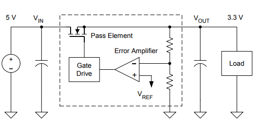
The below image shows the basic Block Diagram for LDO. Main components of an LDO are the Reference voltage, Differential amplifier (error amplifier), and Pass element (field-effect transistor).
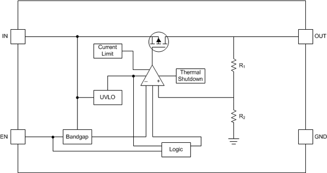
Positive input of the error amplifier monitors the fraction of the output calculated by the ratio of Resistors R1 and R2 while the input at negative pin of the differential amplifier is from a stable voltage reference.
Working of LDO
The working of LDO regulator is just like that of an ordinary linear voltage regulator. LDO has three main components, i.e. pass element, error amplifier, and reference voltage source. Typically pass element is an N-channel or P-channel FET, but can also be an NPN transistor or PNP transistor. As shown in below diagram the input voltage is applied to a pass element, which is an N channel field effect transistor. This field-effect transistor operates in the linear region to reduce the input voltage down to the required output voltage. Error amplifier sense the resulting output voltage and compared it to the reference voltage. The error amplifier changes the FET’s gate to the appropriate operating point to ensure that the output is at the correct voltage. When the input voltage changes, the error amplifier modulates the FET to maintain a constant output voltage. In steady-state operating conditions, an LDO behaves like a simple resistor.
Some LDO regulators are available in fixed and adjustable output voltage versions to adjust the output voltage according to requirement. LDO regulators also have an Enable pin that can be used to turn on or off the regulator; this helps the designers to turn off the regulator and prevent battery usage when not in use.
Important LDO Parameters
Quiescent Current
The term ‘Quiescent’ is defined as “a state or period of inactivity or dormancy.” So the Quiescent current (IQ) is the current drawn by the system in standby mode when light or no load is connected. Quiescent current and shutdown current both are different terms; quiescent current is the current drawn by the system when light or no load is connected while the shutdown current is the current drawn when the device is in the off state, but the battery is still connected to the device.
Power Supply Rejection Ratio (PSRR)
PSRR is defined as the LDO's ability to reject AC elements like ripple voltage. It is expressed by the following formula:
PSRR (dB): 20 log (Vripple (in)/ Vripple (out))
Load Regulation
Load regulation is defined as the circuit’s ability to maintain a specified output voltage under varying load conditions. Load regulation is expressed as:
Load Regulation = ∆Vout/ ∆Iout
Line Regulation
Line regulation is defined as the circuit’s ability to maintain the specified output voltage with varying input voltage. Line regulation is expressed as:
Load Regulation = ∆Vout / ∆Vin
Transient Response
The transient response is defined as the maximum allowable output voltage variation for a load current step change. It is also known as line step response. Transient Response is the function of the output capacitor value (Cout), the equivalent series resistance (ESR) of the output capacitor, the bypass capacitor (Cb) and the maximum load-current (Iout, max). The maximum transient voltage variation is expressed as:
∆Vtr, max = (Iout, max / Cout + Cb) ∆t1 + ∆VESR
Features of LDO
The following are most common features that can be found available in a common LDO regulator. However refer to you particular datasheet to confirm the same since it is not mandatory for every LDO to have all these features.
Under-voltage lockout
When the input voltage drops below the specified input voltage, this function puts the IC in the standby state so that the internal circuit becomes unstable and it doesn’t damage the IC.
Current limit
Excess heat generation by the device during operation can damage and degrade the IC. Current limit function protects the device from excess heat. There are two types of current limit methods: first is foldback type that simultaneously reduces the output current and output voltage, and the second method is current limiter type that reduces the output voltage while keeping the output current constant.
Thermal shut down (TSD)
Sometimes due to unintentional high current load or due to some other reasons, the temperature of the device increases very fast, and it can damage the IC. Thermal shut down function is used to prevent deterioration and destruction of the device because of remarkable ambient temperature rise. When the internal temperature detection circuit detects the high temperature it turns off the output transistor.
Output discharge
When the output transistor is turned off by the internal temperature detection circuit due to high temperature, the terminal voltage of Vout may remain for some time depending on the load capacitance. Output discharge circuit is used to rapidly discharge the charge and drops the Vout terminal voltage to near the IC GND.
Applications
- Cellular Telephones
- Laptop, Notebook, and Palmtop Computers
- Battery-Powered Equipment
- PCMCIA VCC and VPP Regulation/Switching
- Consumer/Personal Electronics
- SMPS Post-Regulator and DC/DC Modules
- High-Efficiency Linear Power Supplies


варочный котел купить