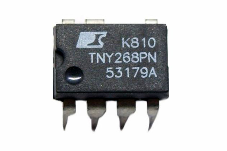
TYN268PN Off-Line Switcher
The TYN268PN is an integrated off-line switching IC that contains the controller and power switch in one package. It needs a minimum number of external components to implement a mains-powered flyback converter.
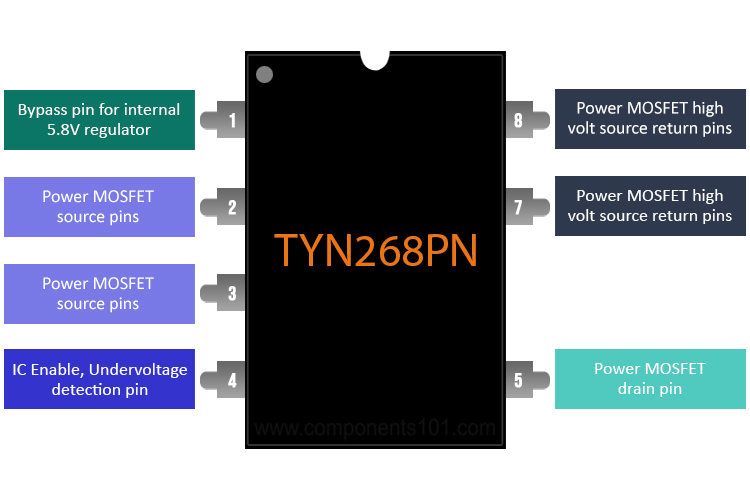
TYN268PN Pinout Description
|
Pin Number |
Pin Name |
Description |
|
1 |
BP |
Bypass pin for internal 5.8V regulator |
|
2, 3 |
S |
Power MOSFET source pins |
|
4 |
EN/UV |
IC enable, undervoltage detection pin |
|
5 |
D |
Power MOSFET drain pin |
|
7, 8 |
S(HV RT) |
Power MOSFET high voltage source return pins |
Features
- Fully integrated off-line switcher
- Up to 23W output power
- 132kHz switching frequency
- Built-in current and overtemperature limit
Note: Complete technical details can be found in the TYN268PN datasheet linked at the end of this page.
Equivalent for TYN238PN
TYN23x series
Other Off-Line Switchers
VIPer32, TYN274
How To Use TYN268PN
Designing an off-line (as in, powered off-line mains voltage) converter has always been a tricky task – apart from calculating various parts parameters, safety must also be taken into account. ICs like the TYN268PN make the job easier by integrating all the necessary control components and the power switch into one IC. Only a few external components are needed, including a transformer and some passives. An example application circuit is shown below.
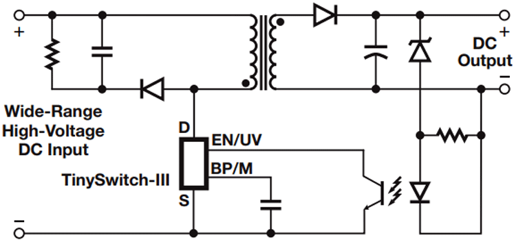
The TYN268PN is treated mostly like a high-voltage power MOSFET connected to the low side of the transformer. Only two extra pins are used – bypass pin for the internal power supply, to which a suitable capacitor must be connected, and the EN/UV pin which also serves as the feedback pin. The feedback network itself is an optocoupler, which is turned on when the output Zener diode exceeds its breakdown voltage. An RC network is connected to the drain of the IC to prevent voltage spikes from damaging the internal power switch. The IC itself has an internal 6.4V Zener diode to clamp the drain-source voltage to safe limits. The current through the switch is internally limited to 500mA.
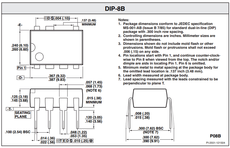
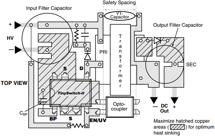
The DIP-8 package in which this IC comes is special as it lacks the seventh pin. This provides some clearance to prevent arcing between pins. The recommended PCB layout is shown in the figure below.
Applications
- Phone chargers
- Off-line power converters
- Battery backup trickle chargers
- High input voltage flyback converters
2D Model and Dimensions