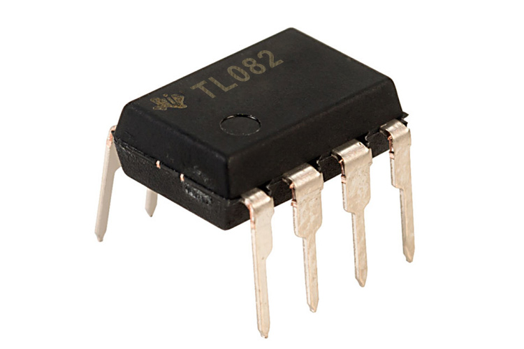
TL082 Wide Bandwidth Dual JFET Input Operational Amplifier
The TL082 Op-Amp is a low cost, high speed, dual JFET input operational amplifier with an internally trimmed input offset voltage. This device requires a low supply current yet maintains a large gain bandwidth product and fast slew rate. In addition, well-matched high voltage JFET input devices provide very low input bias and offset currents.
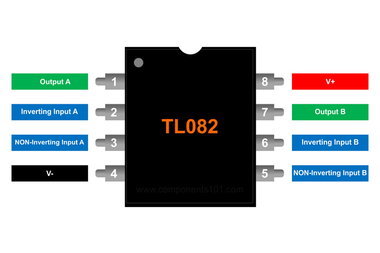
TL082 OpAmp Pinout Configuration
|
Pin Number |
Pin Name |
Pin Description |
|
1 |
Output A |
Output of Op-Amp A |
|
2 |
Inverting Input A |
Inverting Input of Op-Amp A |
|
3 |
NON-Inverting Input A |
Non-Inverting Input of Op-Amp A |
|
4 |
V- |
Ground or Negative (Dual Polarity Supply) |
|
5 |
NON-Inverting Input B |
Non-Inverting Input of Op-Amp B |
|
6 |
Inverting Input B |
Inverting Input of Op-Amp B |
|
7 |
Output B |
Output of Op-Amp B |
|
8 |
V+ |
Supply Voltage |
Features & Specifications
- JFET Input Op-Amp dual Package
- Typical Operating Voltage: +18V to -18V
- Maximum operating Voltage: 36V
- Input Bias Current: 400pA @25°C 8nA @ 70°C
- Common mode Rejection Ratio CMRR: 100dB
- Low Input Bias and Offset Current
- Output Short circuit protection
- Internally Trimmed Offset Voltage: 15 mV
- Low Input Bias Current: 50 pA
- Low Input Noise Voltage: 16nV/√Hz
- Low Input Noise Current: 0.01 pA/√H
- High Slew Rate: 13 V/μs
- Low Supply Current: 3.6 mA
- Low Total Harmonic Distortion: ≤0.02%
- Low 1/f Noise Corner: 50 Hz
- Fast Settling Time to 0.01%: 2 μs
Note: Complete Technical Details can be found in the TL082 IC datasheet given at the end of this page.
TL082 Equivalent Op-Amp
Where to use TL082 Op-Amp
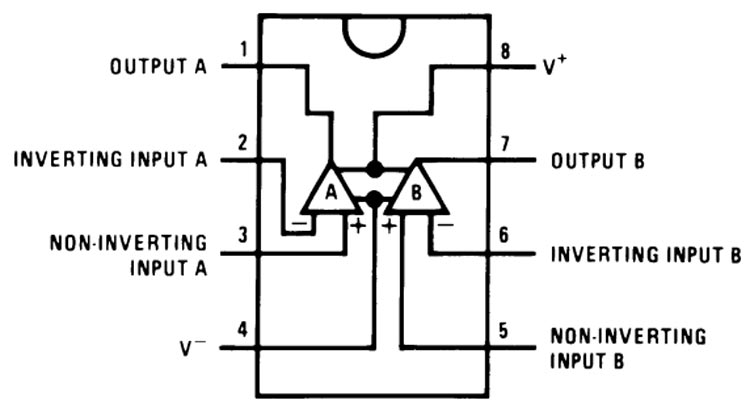
The TL082 is a Dual Package Operational Amplifier, meaning it has two Op-Amps inside it and each Op-Amp can be used independently.
The main distinguishing feature of the TL082 Op-Amp is that they incorporate high-voltage JFET and bipolar transistors which helps the transistor to have very high input impedance and low bias current. Also, this Op-Amp has low noise and harmonic distortion making it an ideal choice for audio pre-amplifiers. Other than that, these amplifiers may be used in applications such as high-speed integrators, fast D/A converters, sample and hold circuits and many other circuits requiring low input offset voltage, low input bias current, high input impedance, high slew rate and wide bandwidth. These devices also exhibit low noise and offset voltage drift. So, if you are looking for an Op-Amp IC with Quad package and JFET driven then this IC might be the right choice for you.
How to use TL082 Op-Amp
TL082 Op-Amp IC can be used for audio pre-amplification and it can provide an edge in terms of sound quality because of its price compared to its specs. As a test, a non-inverting op-amp configuration is shown below.
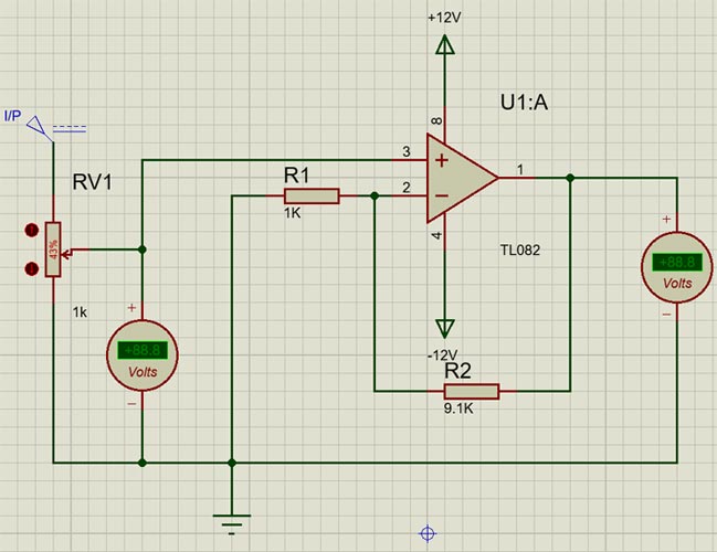
In the above the TL082 Op-amp is configured as a non-inverting configuration. The gain of the op-amp is set to 10. For that we have used a 1K resistor and a 9.1K resistor, as you can see for the simulation, we have used a variable potentiometer. By varying the potentiometer, we can vary the input voltage and the output voltage will also vary, to power the op-amp we have used +12V and -12V supply, as the gain of the op-amp is 10 so if we provide 1V at the input we will get 10V at the output and the simulated circuit shows exactly that.
Applications
- Circuit requiring high input impedance
- Buffer application
- Filter circuits, Voltage followers
- Integrator, Differentiator, Summer, adder, Voltage follower, etc.,
- DC gain blocks
- Comparators (Loop control & regulation)
- Audio Amplifier
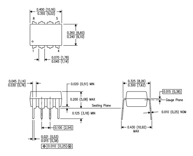
2D Model and Dimensions
If you are designing a PCB or Perf board with this component then the following picture from the Datasheet will be useful to know its package type and dimensions.