LM741 vs LM358

The LM741 and LM358 are classic and popular op-amp designs. The LM358 is a considerably newer part than the LM741, and despite the fact that they are both general-purpose op-amps, there are major differences between them that impact performance and applicability. In this article, we’ll look at the internal and behavioral differences between the two.
Specifications of LM741 and LM358
The first step to understand the differences between the two components is to examine some input specifications.
|
Specification |
LM741 |
LM358 |
|
Supply voltage (max.) |
±22V |
32V (±16V) |
|
Input bias current (max.) |
~200nA |
100nA |
|
Input voltage range (max.) |
±13V (±15V supply) |
0V – (V+ - 1.5V) (30V supply) |
The first noticeable difference is that the specified supply voltage for the LM741 is bipolar, which means both positive and negative supply is needed. The datasheet makes no indication of single supply operation, which we’ll look at in the next section. However, the LM358, states that with a 30V single ended supply, the input can go down to 0V, implying that the input range goes down to the negative supply pin. On the other hand, the upper limit is 1.5V below the positive supply pin.
The difference in the input bias current is also because of the internal structure of the op-amp. Although 100s of nA might not seem like much, 100nA flowing through 10kΩ generates an error voltage of 1mV, which may or may not be much depending on the application.
Note: More technical specifications can be found in the LM741 Datasheet and LM358 Datasheet, linked at the bottom of this page.
Taking a Look at Internal Circuitry of LM741 and LM358
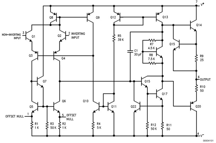
The below figure shows the internal circuit diagram of the LM741.

FIG.1 LM741 INTERNAL CIRCUIT DIAGRAM
The input stage is one feature of this op-amp that explains all three differences from the LM358.
On the LM741, the input stage is made up of a pair of NPN transistors that buffer a PNP transconductance gain stage, a current mirror to split the current evenly between both legs of the differential amplifier, and a current source to supply current to the input stage.
The current mirrors and PNP amplifiers take up two diode drops from the negative supply rail, and the input transistors take up another diode drop, which means that the input should be at least three diode drops (~2V) above the negative supply rail in order to function correctly. So, for single supply operation, the inputs must be maintained above 1.5V to ensure proper operation.
Since only one set of transistors buffers the input stage, the bias current is rather high.
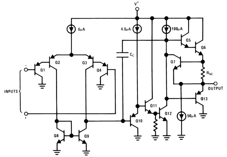
The next figure shows the internal circuit diagram of the LM358.

FIG.2 LM358 INTERNAL CIRCUIT DIAGRAM
Here, the input structure varies greatly from the LM741. The input stage is “twice” buffered, means less bias current. The input transistors are PNP, so even if the input is at 0V, the emitters are still at ~0.6V, which ensures proper operation. Think about it this way – the extra PNP buffer transistors shield the input current mirror from low input voltages, maintaining at least one diode drop across them.
Table Of Major Differences between LM741 and LM358
|
LM741 |
LM358 |
|
Dual supply operation |
Single supply operation |
|
Input common mode range does not include either supply rail, must be at least 2V above and below |
Input common mode range includes negative supply rail, goes up to 1.5V below positive supply rail |
|
Relatively higher bias current |
Relatively lower bias current |
|
The older part, not recommended for new designs |
Easily available and cheap, general-purpose |
|
The single amplifier in a package |
Dual amplifiers in a single package, quad available |
Conclusion
Both the LM741 and LM358 are classic and easily available general-purpose op-amps, but when the features are compared, the LM358 is a clear winner in all categories.


