DAC0832 – 8 bit Digital to Analog Converter

As the name itself points out ‘DAC0832’ is a DAC chip or Digital to Analog Conversion IC. The device is from DAC0830 series that are 8-bit members of a family of microprocessor-compatible DACs. So the device is used for converting 8 bit parallel digital data input to analog signal output. The chip is designed with CMOS technology to achieve low power consumption and low output leakage current errors. The design also includes special circuitry that provides TTL logic input voltage level compatibility. Double buffering of the device allows outputting a voltage corresponding to one digital word while holding the next digital word. This also permits the simultaneous updating of any number of DACs.
DAC0832 also designed with silicon-chromium R-2R resistor ladder network which divides the reference current and provides the circuit with excellent temperature tracking characteristics (0.05% of Full Scale Range maximum linearity error over temperature).
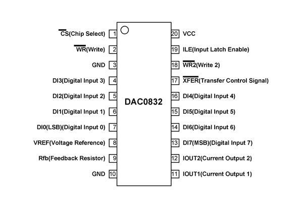
Pin Configuration
DAC0832 is a twenty pin device and description for each pin is given below.
|
Pin |
Name |
Description |
|
1 |
CS |
Chip Select (Active Low) needed to be grounded for enabling the chip |
|
2 |
WR |
Write (Active Low) needed to be grounded for successful data transmission |
|
3 |
GND |
Ground |
|
4 |
DI3 |
Digital Input 3 will take data for conversion |
|
5 |
DI2 |
Digital Input 2 will take data for conversion |
|
6 |
DI1 |
Digital Input 1 will take data for conversion |
|
7 |
DI0(LSB) |
Digital Input 0(Least Significant Bit) will take data for conversion |
|
8 |
VREF |
Voltage Reference for the chip is given at this pin |
|
9 |
Rfb |
Feedback Resistor will be connected to this pin |
|
10 |
GND |
Ground |
|
11 |
IOUT1 |
Current Output 1 will give analog output after conversion |
|
12 |
IOUT2 |
Current Output 2 will give analog output after conversion |
|
13 |
DI7(MSB) |
Digital Input 7(Most Significant Bit) will take data for conversion |
|
14 |
DI6 |
Digital Input 6 will take data for conversion |
|
15 |
DI5 |
Digital Input 5 will take data for conversion |
|
16 |
DI4 |
Digital Input 4 will take data for conversion |
|
17 |
XFER |
Transfer Control Signal (Active Low) |
|
18 |
WR2 |
Write 2 (Active Low) |
|
19 |
ILE |
Input Latch Enable pin needed to be high for successful data transmission |
|
20 |
VCC |
Positive Power Supply |
DAC0832 Features and Electrical Characteristics
- 8 bit parallel digital data input
- Operates from single power supply
- Direct interface to all popular microprocessors
- Operates ‘STAND ALONE’ (without microprocessor or microcontroller) if desired
- Double-buffered, single-buffered or flow-through digital data inputs
- Digital inputs are TTL and CMOS compatible
- Can be used in the voltage switching mode
- Works with ±10V reference
- Easy interchange and pin-compatible with 12-bit DAC1230 series
- Linearity specified with zero and full scale adjust only
- Power supply voltage range: +5V to +15V
- Low power consumption: 20 mW
- Maximum Power dissipation: 500 mW
- Operating temperature range: 0ºC to +75ºC
- Maximum ESD protection: 800V
Similar DAC Chips
DAC0830/DAC0831, DAC0807, DAC0806, DAC0800, DAC0802, AD557
DAC0832 Overview
DAC0832 IC basically used in applications where an 8 bit digital data needed to be converted to analog value. The device is specifically designed for it to be interfaced directly with the 8080, 8048, 8085, Z80, and other popular microprocessors. The device is available in the market for low cost and can be easily worked with.
How to use DAC0832
Before going for working let us consider functional diagram of the IC DAC0832 as shown below.
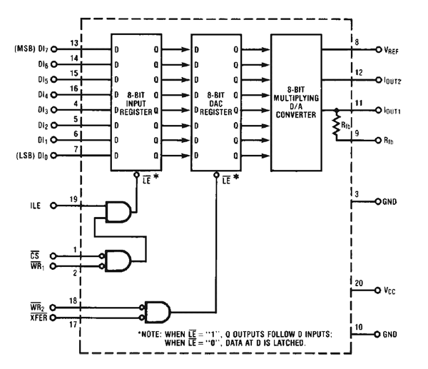
Based on the functional diagram we can write,
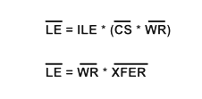
As mentioned in the functional diagram in both cases
In the first case for
- ILE = HIGH
- CS = LOW
- WR = LOW
In the second case for
- WR = LOW
- XFER = LOW
All these control pins need to be setup appropriately as mentioned above for successful DAC conversion of the device.
Now for understanding the working let us consider the example application circuit given in the datasheet. We can use the circuit to develop applications without worry as the circuit is tested working.
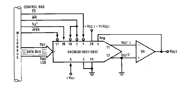
In circuit:
- For working of device DAC0832 we have connected a voltage source of 15V as shown in diagram.
- Eight digital inputs are given to the chip and are supposed to be in order from MSB to LSB.
- Vref is optional but remember the maximum output voltage cannot go higher than Vref
Working
DAC0832 takes in parallel 8 bit data from a microcontroller or microprocessor and converts that data in to analog signal at the output. This analog signal is the current quantity that is directly proportional to the input digital value and this current parameter needed to be converted in to voltage parameter for further use. So to convert the current parameter in to voltage parameter we will use op-amp circuit as shown in circuit diagram. This op-amp circuit is called current-to-voltage converter.
The analog voltage output from the op-amp circuit is in direct relation with inputted digital value and hence DAC conversion with DAC0832 is achieved.
Applications
- Microprocessor interface
- Analog and digital circuits
- Electrical measurements
- Audio conversion
- Hobbyist applications
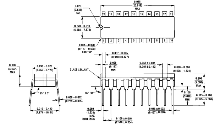
2D-Model
All dimensions are in inches [millimeter measurements in brackets]