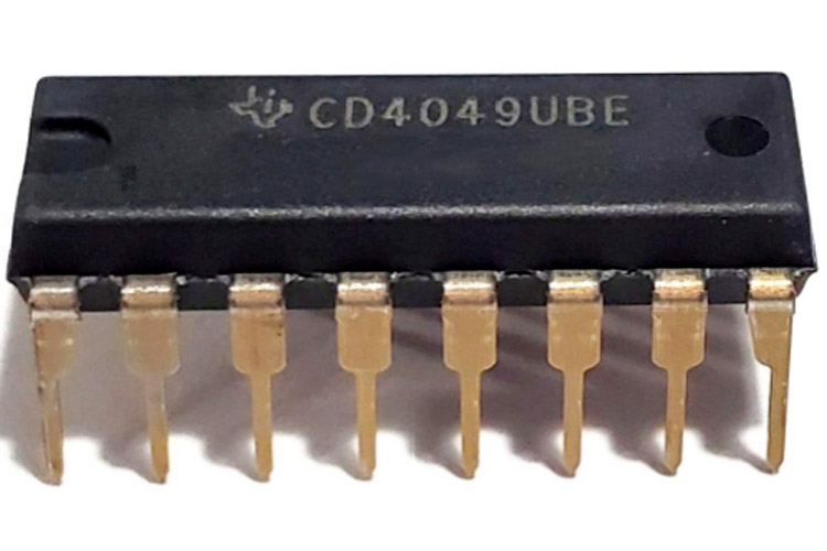
CD4049 Hex Buffer Converter (NOT Gate) IC
CD4049 Hex Buffer Converter (NOT Gate) IC is an inverting buffer IC consisting of 6 individual NOT gates present inside. The NOT gate IC is intended for use as CMOS to DTL or TTL converters and can drive up to 2 DTL or TTL devices at a time.
Features and Specifications
This section mentions some of the important features and specifications of the CD4049 IC.
- Operating Voltage: 3V - 18V DC
- Current consumption(max): 50mA
- High Sink Current for Driving 2 TTL Loads
- Maximum low-level output Voltage: 0.5V at 5V Vcc
- Minimum high-level output voltage: 4.95 at 5V Vcc
Note: More technical information can be found in the CD4049 Datasheet, linked at the bottom of this page.
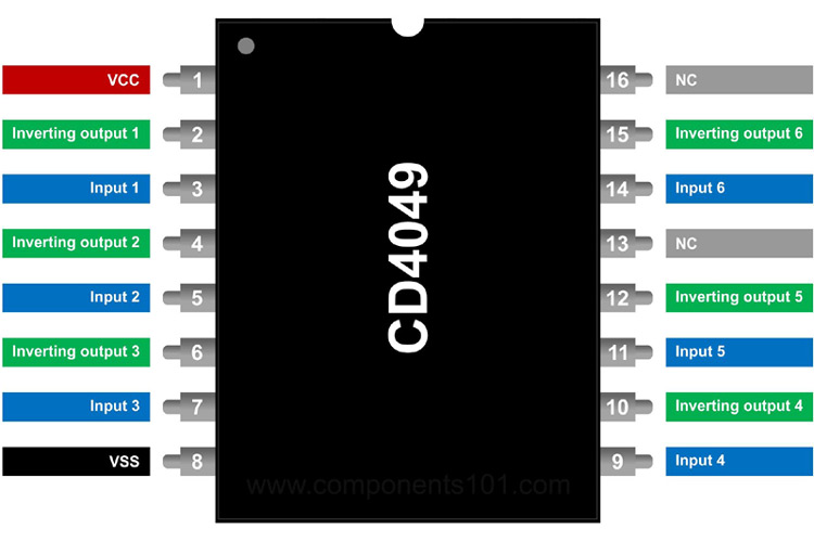
CD4049 Pinout Configuration
The CD4049 IC has 16 pins for Input and Output for inverting the signals. The table below describes the pin configuration of the NOT gate IC.
|
Pin Number |
Pin Type |
Description/Direction |
|
1 |
VCC |
Positive input supply |
|
2 |
G |
Inverting output 1 |
|
3 |
A |
Input 1 |
|
4 |
H |
Inverting output 2 |
|
5 |
B |
Input 2 |
|
6 |
I |
Inverting output 3 |
|
7 |
C |
Input 3 |
|
8 |
VSS |
Negative Supply |
|
9 |
D |
Input 4 |
|
10 |
J |
Inverting output 4 |
|
11 |
E |
Input 5 |
|
12 |
K |
Inverting output 5 |
|
13 |
NC |
No connection |
|
14 |
F |
Input 6 |
|
15 |
L |
Inverting output 6 |
|
16 |
NC |
No connection |
Working Principle and Internal Schematic
A NOT gate provides an inverting output corresponding to the given input. It is widely used in high to low-level converters and has many more applications.
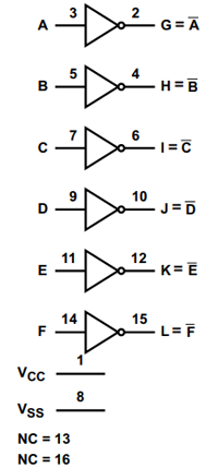
The image above shows how NOT gates are connected in the CD4049 IC. VCC and VSS are the power pins and are to be connected to the VCC and the ground of the power source. NC pins are to be left floating. Here, input pin A is connected to the output pin G; HIGH signal to pin A will provide us a LOW signal at pin G and if a LOW signal is provided to pin A, we will obtain a HIGH signal at pin G. That is what inverting a given signal is. The same follows with pin B-H, C-I, D-J, E-K, F-L respectively.
Typical Application Circuit and Output Table
Below is a typical application circuit shown using a NOT gate to glow an LED. The logic signal depending upon its state (HIGH or LOW) provides an inverting output.
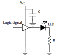
The table below gives a clear picture of the working of a NOT gate. Whenever a HIGH input signal is given to A, B, C, D, E, F pins of the CD4049 IC the output we will receive is LOW on G, H, I, J, K, L respectively.
|
Input Signal (A, B, C, D, E, F) |
Output Signal (G, H, I, J, K, L) |
|
HIGH |
LOW |
|
LOW |
HIGH |
Alternatives
7404, 74LS04
Available packages
PDIP(16), SOIC(16), SO(16), TSSOP(16)
Applications
Here are some of the applications of CD4049 Hex Buffer Converter (NOT Gate) IC.
- CMOS to DTL or TTL Hex Converters
- CMOS Current Sink or Source Drivers
- CMOS High-to-Low Logic Level Converters
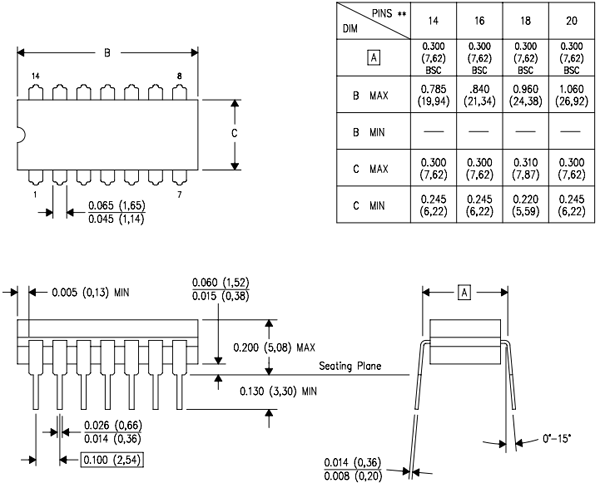
2D Model
Below is the 2D model of the IC along with its dimensions in inches (millimeters). The following information can be used while designing custom footprints of the IC, which can be used for PCB designing and CAD modelling.