AD8310 Logarithmic Amplifier
The AD8310 is a complete dc to 440 MHz demodulating logarithmic amplifier with a very fast voltage-mode output, capable of driving up to 25 mA into a grounded load in under 15 ns. It uses the progressive compression (successive detection) technique to provide a dynamic range of up to 95 dB to ±3 dB law conformance or 90 dB to a ±1 dB error bound up to 100 MHz. It is extremely stable and easy to use, requiring no significant external components.
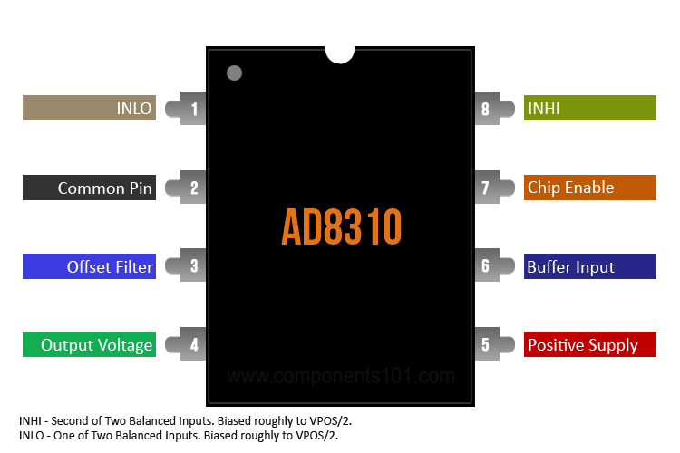
AD8310 Pinout Configuration
|
Pin Number |
Pin Name |
Pin Description |
|
1 |
INLO |
One of Two Balanced Inputs. Biased roughly to VPOS/2. |
|
2 |
COMM |
Common Pin. Usually grounded. |
|
3 |
OFLT |
Offset Filter Access. Nominally at about 1.75 V. |
|
4 |
VOUT |
Low Impedance Output Carries a 25 mA maximum load. |
|
5 |
VPOS |
Positive Supply. 2.7 V to 5.5 V at 8 mA quiescent current. |
|
6 |
BFIN |
Buffer Input. Used to lower post-detection bandwidth. |
|
7 |
ENBL |
CMOS Compatible Chip Enable. Active when high. |
|
8 |
INHI |
Second of Two Balanced Inputs. Biased roughly to VPOS/2. |
Features & Specifications
- Multistage demodulating logarithmic amplifier
- Voltage output, rise time <15 ns
- High current capacity: 25 mA into grounded RL
- 95 dB dynamic range: –91 dBV to +4 dBV
- Single supply of 2.7 V min at 8 mA type
- DC to 440 MHz operation, ±0.4 dB linearity
- Slope of +24 mV/dB, intercept of –108 dBV
- Highly stable scaling over-temperature
- Fully differential dc-coupled signal path
- Max Supply Voltage 7.5V
- 100 ns power-up time, 1 mA sleep current
- Input Power (re 50 Ω), Single-Ended 18 dBm
- Maximum Junction Temperature 125°C
- Internal Power Dissipation 200 mW
Note: Complete technical information can be found in the AD8310 datasheet linked given at the bottom of the page.
Equivalent ICs
TL441, MAX4206
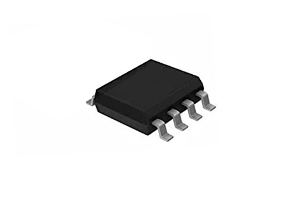
Available Packages
8-Lead MSOP
How to use AD8310 Logarithmic Amplifier IC?
Logarithmic amplifiers perform a more complex operation than classical linear amplifiers, and their circuitry is significantly different. A good grasp of what log amps do and how they do it can help users avoid many pitfalls in their applications. The essential purpose of a log amp is not to amplify (though amplification is needed internally) but to compress a signal of a wide dynamic range to its decibel equivalent. It is, therefore, a measurement device. An even better term might be a logarithmic converter because the function is to convert a signal from one domain of representation to another via a precise nonlinear transformation:
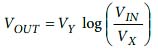
where: VOUT is the output voltage.
VY is the slope voltage. The logarithm is usually taken to base ten, in which case VY is also the volts-per-decade.
VIN is the input voltage. VX is the intercept voltage.
The below circuit shows how the connections are needed for most applications. A supply voltage between 2.7 V and 5.5 V is applied to VPOS and is decoupled using a 0.01 μF capacitor close to the pin. Optionally, a small series resistor can be placed in the power line to give additional filtering of power-supply noise. The ENBL input, which has a threshold of approximately 1.3 V, should be tied to VPOS when this feature is not needed.
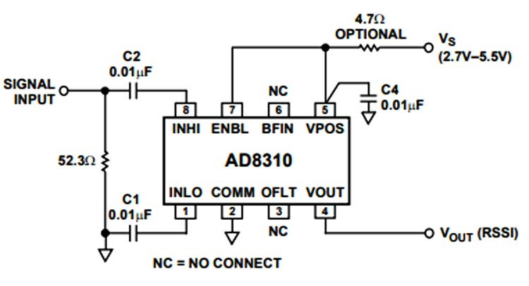
While the AD8310’s input can be driven differentially, the input signal is, in general, single-ended. C1 is tied to the ground, and the input signal is coupled in through C2. Capacitor C1 and Capacitor C2 should have the same value to minimize start-up transients when the enable feature is used; otherwise, their values need not be equal. The 52.3 Ω resistor combines with the 1.1 kΩ input impedance of the AD8310 to yield a simple broadband 50 Ω input match. An input matching network can also be used.
Applications
- Conversion of signal level to decibel form
- Transmitter antenna power measurement
- Receiver signal strength indication (RSSI)
- Low-cost radar and sonar signal processing
- Network and spectrum analyzers
- Signal-level determination down to 20 Hz
- True-decibel ac mode for mustimeters
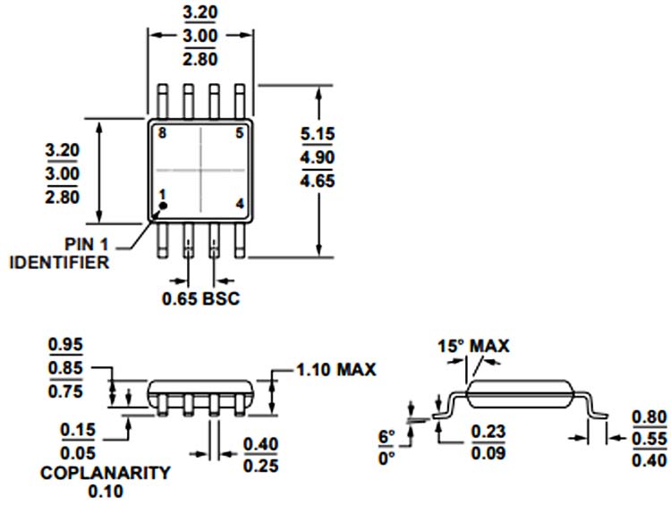
2D Model and Dimensions
If you are designing a PCB or Perf board with this component then the following picture from the Datasheet will be useful to know its package type and dimensions.