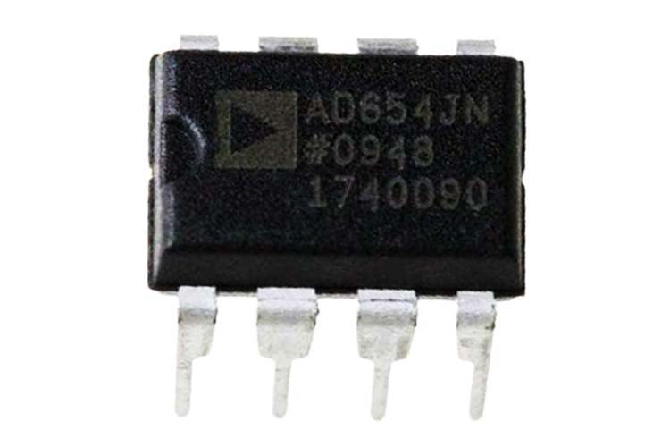
AD654 Voltage-to-Frequency Converter IC
The AD654 is a monolithic Voltage Frequency converter consisting of an input amplifier, a precision oscillator system, and a high current output stage. A single RC network is all that is required to set up any full scale (FS) frequency up to 500 kHz and any FS input voltage up to ± 30 V. Linearity error is only 0.03% for a 250 kHz FS, and operation is guaranteed over an 80 dB dynamic range. The overall temperature coefficient (excluding the effects of external components) is typically ±50 ppm/°C. The AD654 operates from a single supply of 5 V to 36 V and consumes only 2.0 mA quiescent current. The low drift (4 µV/°C types) input amplifier allows operation directly from small signals such as thermocouples or strain gauges while offering a high (250 MΩ) input resistance. Unlike most V/F converters, the AD654 provides a square-wave output and can drive up to 12 TTL loads, optocouplers, long cables, or similar loads which make it suitable for many modern-day applications.
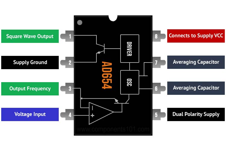
AD654 Pinout Configuration
|
Pin Number |
Pin Name |
Description |
|
1 |
Fout |
Square Wave Output |
|
2 |
Logic Common |
Connects to Supply Ground |
|
3 |
RT |
Adjust Output Frequency |
|
4 |
+Vin |
Voltage Input |
|
5 |
-VS |
-Vcc of Dual Polarity Supply |
|
6 |
CT |
Averaging Capacitor |
|
7 |
CT |
Averaging Capacitor |
|
8 |
+VS |
Connects to Supply Vcc |
Features & Specifications
- Low Cost
- Single or Dual Supply, 5 V to 36 V.\
- Full-Scale Frequency Up to 500 kHz
- Minimum Number of External Components Needed
- Versatile Input Amplifier
- Positive or Negative Voltage Modes
- Negative Current Mode
- High Input Impedance,
- Low Drift Low Power: 2.0 mA Quiescent Current
- Low Offset: 1 mV
- Max Supply Voltage 36V
- Max Input Voltage -300mV to Supply Voltage.
- Maximum Output Current 50mA
- Storage Temperature Range −65°C to +150°C
- Full Scale Calibration Error -10% to +10%
Note: Complete Technical Details can be found in the AD654 datasheet given at the end of this page.
Equivalent ICs
KA331, LM331
Available Packages for AD654 V/F IC
DIP-8, SOIC-8
How to use AD654 V/F Converter IC
Configuring this IC to a Voltage to frequency is very easy as it requires a handful of components to do so. An operational amplifier serves as the input stage, its purpose is to convert and scale the input voltage signal to a drive current in the NPN follower. Optimum performance is achieved when at the full-scale input voltage, a 1 mA drive current is delivered to the current-to-frequency converter (an astable multivibrator). The drive current provides both the bias levels and the charging current to the externally connected timing capacitor. This “adaptive” bias scheme allows the oscillator to provide low nonlinearity over the entire current input range of 100 nA to 2 mA. The square wave oscillator output goes to the output driver which provides a floating base drive to the NPN power transistor. This floating drive allows the logic interface to be referenced to a level other than –V.
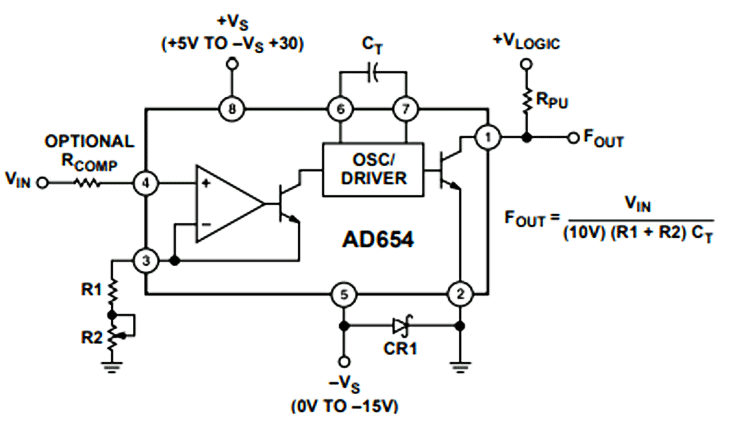
The above figure shows a basic circuit of the Voltage to Frequency Converter circuit using the AD654 Voltage to Frequency Converter IC. There are many more applications available for this device, you can check out the datasheet for more information and example circuits. The AD654 can accommodate a wide range of negative input voltages with proper selection of the scaling resistor.
Applications
- Two-Wire Temperature-to-Frequency Converter
- Optoisolator Interface for HV Systems
- AD654 With Stand-Alone Frequency Counter
- LED Display Driver
- AD654 VFC as an ADC
- Frequency Doubler
- Analog to Digital Converter
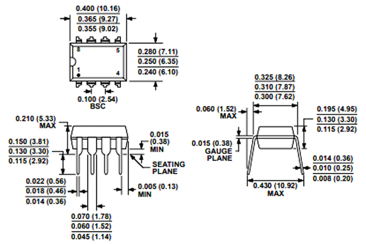
2D Model and Dimensions
If you are designing a PCB or Perf board with this component then the following picture from the Datasheet will be useful to know its package type and dimensions.