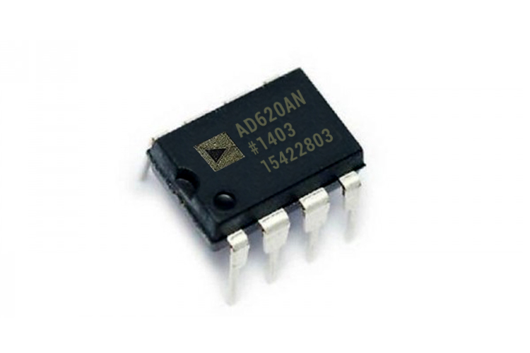
AD620 Low-Power Instrumentation Amplifier
The AD620 is a low-cost, low-power, high accuracy instrumentation amplifier that requires only one external resistor to set gains of 1 to 10,000. Furthermore, the AD620 features 8-lead SOIC and DIP packaging that is smaller than discrete designs and offers lower power (only 1.3 mA max supply current), making it a good fit for battery-powered, portable (or remote) applications.
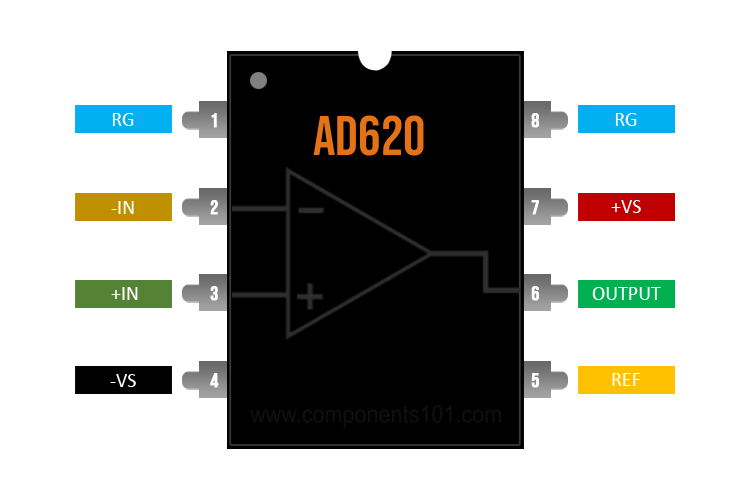
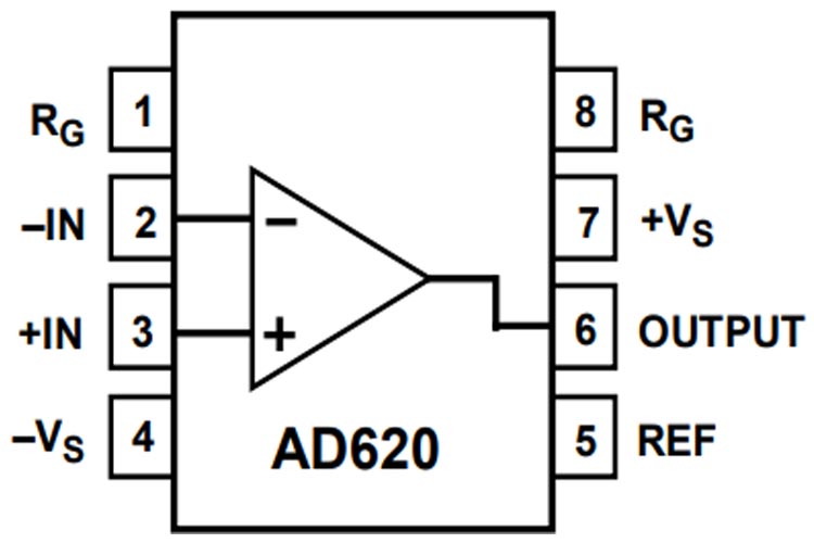
AD620 Amplifier Pinout Configuration
|
Pin Number |
Pin Name |
Description |
|
1 |
RG |
External Gain Set Resistor |
|
2 |
-IN |
Inverting Input of op-Amp A |
|
3 |
+IN |
Non-Inverting Input of op-Amp A |
|
4 |
-VS |
Ground or Negative (Dual Polarity Supply) |
|
5 |
REF |
Reference Input |
|
6 |
OUTPUT |
Output of the op-amp |
|
7 |
+VS |
VCC of the Supply |
|
8 |
RG |
External Gain Set Resistor |
Features & Specifications
- Gain set with one external resistor (Gain range 1 to 10,000)
- Wide power supply range (±2.3 V to ±18 V)
- Higher performance than 3 op amp IA designs
- Available in 8-lead DIP and SOIC packaging
- Low power, 1.3 mA max supply current
- 50 μV max, input offset voltage
- .6 μV/°C max, input offset drift
- 1.0 nA max, input bias current
- 100 dB min common-mode rejection ratio (G = 10)
- Low noise 9 nV/√Hz @ 1 kHz, input voltage noise
- 0.28 μV p-p noise (0.1 Hz to 10 Hz)
- 120 kHz bandwidth (G = 100)
- 15 μs settling time to 0.01%
Note: Complete technical details can be found in the AD620 datasheet given at the end of this page.
AD620 Equivalent
AD8221, AD8222, AD8226, AD8228, AD8295
AD620 Theory of Operation
The AD620 is a monolithic instrumentation amplifier based on a modification of the classic three op-amp approach. Absolute value trimming allows the user to program gain accurately (to 0.15% at G = 100) with only one resistor. Monolithic construction and laser wafer trimming allow the tight matching and tracking of circuit components, thus ensuring the high level of performance inherent in this circuit. The circuit below shows how the basic construction works.
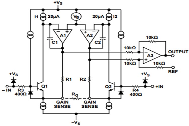
The value of RG determines the transconductance of the preamp stage. As RG is reduced for larger gains, the transconductance increases asymptotically to that of the input transistors. This has three important advantages:
- Open-loop gain is boosted for increasing programmed gain, thus reducing gain-related errors.
- The gain-bandwidth product (determined by C1 and C2 and the preamp transconductance) increases with programmed gain, thus optimizing frequency response.
- The input voltage noise is reduced to a value of 9 nV/√Hz, determined mainly by the collector current and base resistance of the input devices.
The internal gain resistors, R1 and R2, are trimmed to an absolute value of 24.7 kΩ, allowing the gain to be programmed accurately with a single external resistor.
The gain equation is then

Where to use AD620
The AD620 is a Single Package Operational Amplifier, meaning it has one Op-Amps inside it, this op-amp has many features that we will discuss later.
The AD620, with its high accuracy of 40 ppm maximum nonlinearity, the low offset voltage of 50 μV max, and offset drift of 0.6 μV/°C max, is ideal for use in precision data acquisition systems, such as weight scales and transducer interfaces. Furthermore, the low noise, low input bias current, and low power of the AD620 make it well suited for medical applications, such as ECG and non-invasive blood pressure monitors.
The low input bias current of 1.0 nA max is made possible with the use of Superϐeta processing in the input stage. The AD620 works well as a preamplifier due to its low input voltage noise of 9 nV/√Hz at 1 kHz, 0.28 μV p-p in the 0.1 Hz to 10 Hz band, and 0.1 pA/√Hz input current noise. Also, the AD620 is well suited for multiplexed applications with its settling time of 15 μs to 0.01%, and its cost is low enough to enable designs with one in-amp per channel.
How to use AD620 Instrumentation Amplifier
We can use this IC for audio pre-amplification, Weigh scales, ECG and medical instrumentation, and more, it can provide an edge in terms of sound quality because of its price compared to its specs. As a test, a non-inverting op-amp configuration is shown below,
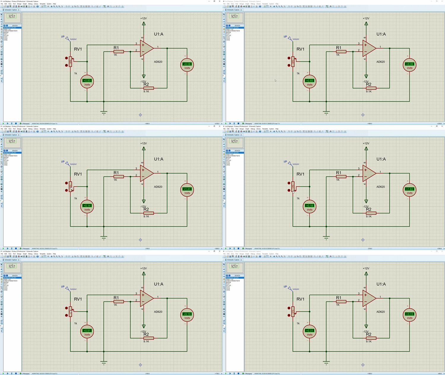
In the above, the AD620 is configured as a non-inverting configuration. The gain of the op-amp is set to 10. For that we have used a 1K resistor and a 9.1K resistor, as you can see for the simulation we have used a variable potentiometer be varying the potentiometer we can vary the input voltage and the output voltage will also vary, to power the op-amp we have used +12V and -12V supply, as the gain of the op-amp is 10 so if we provide 1V at the input we will get 10V at the output the simulated circuit shows exactly that.
Applications
- Weigh scales
- ECG and medical instrumentation
- Transducer interface
- Data acquisition systems
- Industrial process controls
- Battery-powered and portable equipment
2D Model and Dimensions
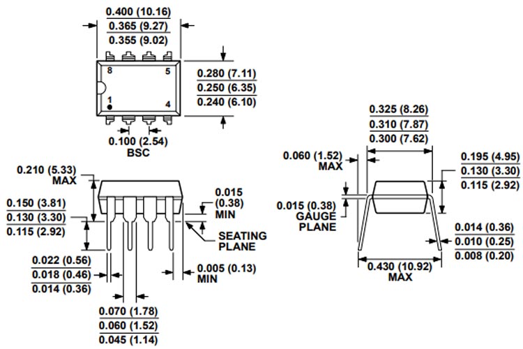
If you are designing a PCB or Perf board with this component then the following picture from the Datasheet will be useful to know its package type and dimensions.
