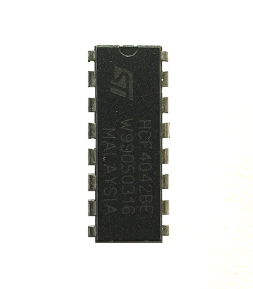
CD4042 - Quad Flip-Flop IC

Pin Configuration
|
Pin No. |
Pin Name |
Description |
|
1 |
Q4 |
Output of Data Pin D4 |
|
2 |
Q1 |
Output of Data Pin D1 |
|
3 |
Q1’ |
Inverting Output of Data Pin D4 |
|
4 |
D1 |
Data input of flip flop 1 |
|
5 |
Clock |
Clock input of the IC |
|
6 |
Polarity |
Used to change the Rising time of the output |
|
7 |
D2 |
Data input of flip flop 2 |
|
8 |
Vss |
Ground |
|
9 |
Q2’ |
Inverting Output of Data Pin D2 |
|
10 |
Q2 |
Output of Data Pin Data Pin D2 |
|
11 |
Q3 |
Output of Data Pin Data Pin D3 |
|
12 |
Q3’ |
Inverting Output of Data Pin D3 |
|
13 |
D3 |
Data input of flip flop 3 |
|
14 |
D4 |
Data input of flip flop 4 |
|
15 |
Q4’ |
Inverting Output of Data Pin D4 |
|
16 |
Vdd |
ICs positive input |
Features
- Common Clock Input
- Low power TTL Compatible
- It gives normal and inverting Output (Q and Q’)
- Four Flip-flop Inside
- Available in both DIP and SOP Package
- Clock Polarity based controlled output
- Quiescent current specified up to 20v
Technical Specifications
- Input Supply voltage: 3v to 20v
- DC Input Current: ± 10 mA
- Input Capacitance: 5 to 7.5 pF
- Setup Time: 25 to 50ns (vary according to voltage)
- Hold Time: 50 to 120ns (vary according to voltage)
- Storage Temperature -65 to +150 °C
- Operating Temperature -55 to 125 °C
Note: Complete technical information can be found in the CD4042 Datasheet linked at the bottom of this page.
CD4042 Equivalent ICs
74ALS175, 74LS74, HEF4013B, 74AHC74, 4013, 7475, 74377, NTE74C74
Where to Use CD4042?
CD4042 IC used for the various purpose in electronics, the IC can be used for data transfer, bounce elimination switch, Buffer storage, holding registers, or for giving general digital logic. This IC doesn’t require many external components. We can also change the rise and fall time of Output by setting Polarity terminal.
How to Use CD4042?
There are four Flip-flops present inside 4042 IC, each strobe by a common clock. It has four Data input pins, each of them have two output inverting and non-inverting. Information present at Data input pin is transferred to the outputs of Q and Q’ based on the clock and polarity input. The truth table of the IC is given below:
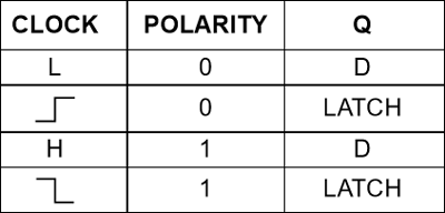
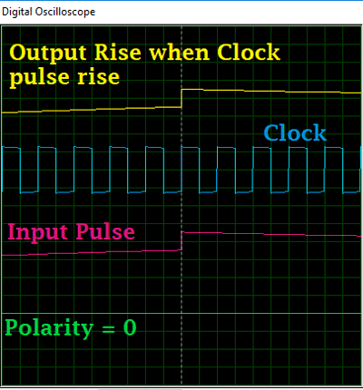
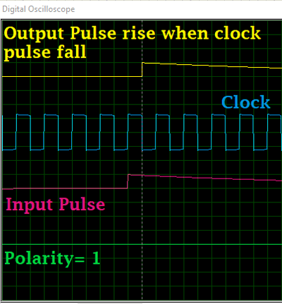
Polarity changes the rising and fall time of the Output. For understanding this, see the waveform below:
When Polarity set to Low, on giving high pulse, the output waveform will rise when the clock pulse is in rising state
When Polarity set to High, on giving high pulse the output waveform will rise when the clock pulse is in falling state
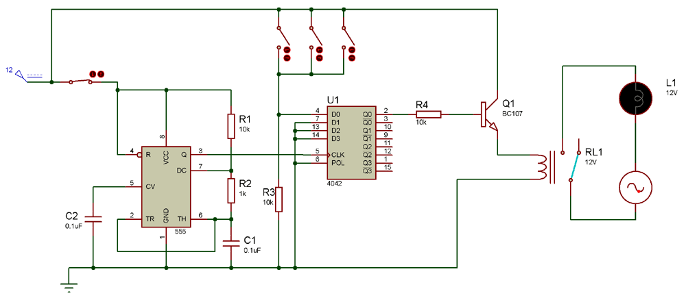
Now, the circuit given below shows that how we can use CD4042 IC for making an electronic circuit. This is the multi-switch circuit which is taking input from the Data pin D0. In this circuit, we are using only one Flip-flop of the IC. As the Data input is High the LED will glow until or we can say the Output Q will be HIGH until the Data input goes Low. We can control the Output from any of the Four Switches preset in the circuit.
Applications
- Bounce elimination switch
- Buffer Storage
- Data transfer
- Holding Register
- General Digital Logic
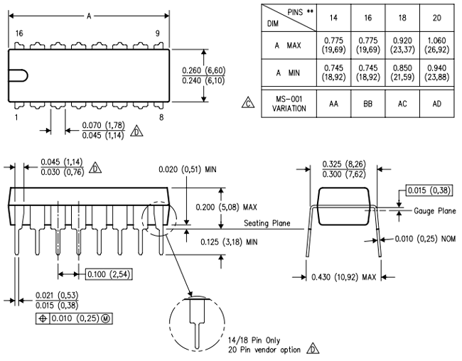
2D-model and Dimensions