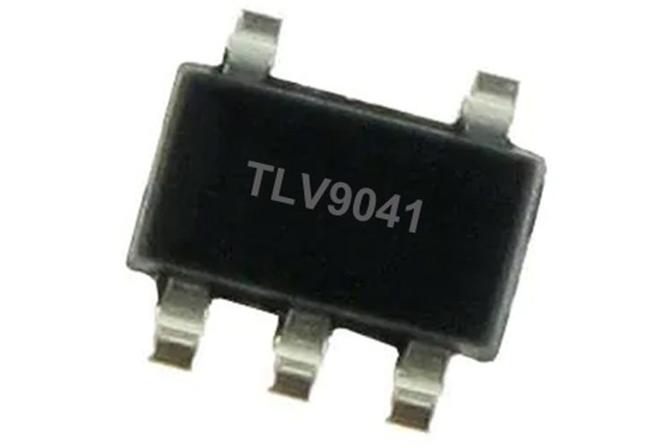
TLV9041 Ultra Low Voltage Op Amp IC
The low-power TLV9041 includes a single ultra-low-voltage (1.2 V to 5.5 V) operational amplifier (op-amps) with rail-to-rail input and output swing capabilities. The TLV9041 enables power savings both with its low quiescent current (10 µA, typ.) and the ability to operate at supply voltages as low as 1.2 V, making it one of the few amplifiers in the industry capable of 1.5-V coin cell applications.
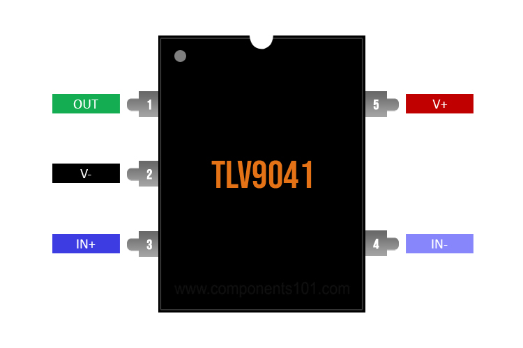
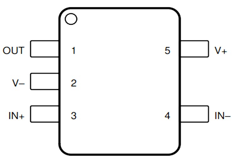
TLV9041 IC Pinout Configuration
|
Pin Number |
Pin Name |
Pin Description |
|
1 |
Out |
Output of Op-Amp |
|
2 |
V- |
Ground or Negative (Dual Polarity Supply) |
|
3 |
Inverting Input |
Inverting Input of Op-Amp |
|
4 |
Non-Inverting Input |
Non-Inverting Input of Op-Amp |
|
5 |
V+ |
Supply Voltage |
Features & Specifications
- Low power CMOS amplifier for cost-optimized applications
- Operational from supply voltage as low as 1.2 V
- Low input bias current: 1-pA typical, 12-pA maximum
- Low quiescent current: 10 µA/ch
- Low integrated noise of 6.5 µVp-p in 0.1 Hz – 10 Hz
- Rail-to-rail input and output
- High gain-bandwidth product: 350 kHz
- Thermal noise floor: 64 nV/√Hz
- Low input offset voltage: ±0.6 mV
- Unity-gain stable
- Robustly drives 100 pF of load capacitance
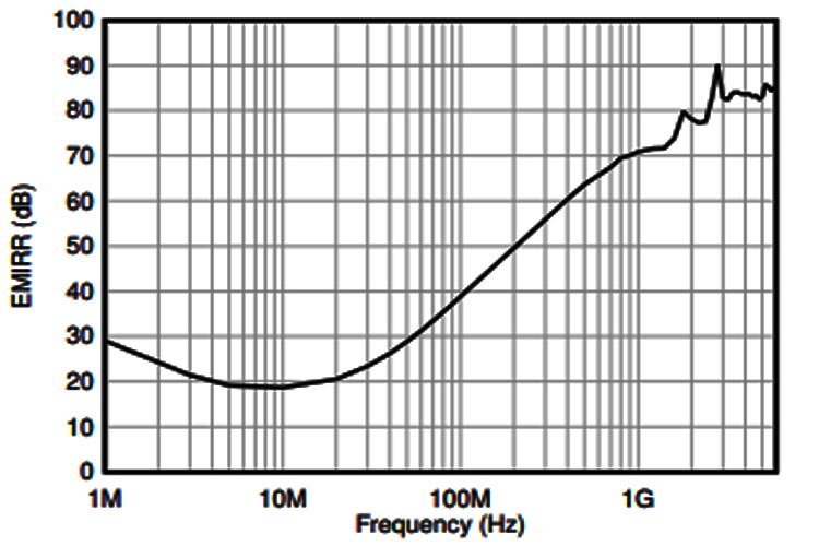
- Internal RFI and EMI filtered input pins
- Wide specified temperature range: –40°C to 125°C
Note: Complete technical details can be found in the TLV9041 datasheet given at the end of this page.
TLV9041 Equivalent
TL074, TL072, TLV9042, TLV9044
Where to use TLV9041
The TLV9041 is a Single Package Operational Amplifier, meaning it has a single Op-Amps inside it and can be used in many different applications.
The main distinguishing feature of the TLV9041 Op-Amp is that they are ultra-low distortion, low-noise operational amplifiers fully specified for audio applications. A cost-effective solution for space-constrained applications such as smoke detectors, wearable electronics, and small appliances where low-voltage operation and high capacitive-load drive are required. The capacitive-load drive of the TLV9041 is 500 pF, and the resistive open-loop output impedance makes stabilization easier with much higher capacitive loads. These op-amps are designed specifically for low-voltage operation (1.2 V to 5.5 V) with performance specifications similar to the TLV600x devices, and the ability to operate at supply voltages as low as 1.2 V, making it one of the few amplifiers in the industry capable of 1.5-V coin cell applications. Further power savings can be achieved using the shutdown mode that allows the amplifiers to be switched off and enter into a standby mode with typical current consumption of less than 150 nA. These devices offer a cost-effective amplifier solution for power and space-constrained applications such as battery-powered IoT devices, wearable electronics, and personal electronics where low-voltage operation is crucial.
The device also delivers excellent AC performance with a gain bandwidth of 350 kHz and a high cap load drive of 100 pF, enabling designers to achieve both improved performance and lower power consumption
Space-saving micro-size packages, such as X2QFN and WSON, are offered for all channel variants (single, dual, and quad), along with industry-standard packages such as SOIC, VSSOP, TSSOP, and SOT-23 packages.
Special Features of TLV9041 IC
The TLV9041 is a low-power, rail-to-rail input, and output op-amps. These devices operate from 1.2 V to 5.5 V, and are unity-gain stable, and are designed for a wide range of general-purpose applications. The input common-mode voltage range includes both rails and allows the TLV9041 devices to be used in any single-supply application. Rail-to-rail input and output swing significantly increases dynamic range, especially in low-supply applications, and makes them suitable for driving sampling analog-to-digital converters (ADCs). Other than that, this IC has many different some of which are discussed below.
The TLV9041 IC can operate from 1.2 V to 5.5 V. In addition, many specifications apply from –40°C to 125°C. The input common-mode voltage range of the TLV9041 IC extends to either supply rail. This is true even when operating at the ultra-low supply voltage of 1.2 V, all the way up to the standard supply voltage of 5.5 V, which means it is a rail-to-rail op-amp.
The TLV9041 is designed to be used in applications where driving a capacitive load is required. As with all operational amplifiers, there may be specific instances where the TLV9041 can become unstable. The particular operational amplifier circuit configuration, layout, gain, and output loading are some of the factors to consider when establishing whether or not an amplifier is stable in operation.
Overload recovery is defined as the time required for the operational amplifier output to recover from a saturated state to a linear state. The output devices of the operational amplifier enter a saturation region when the output voltage exceeds the rated operating voltage, because of the high input voltage or high gain. Once one of the output devices enters the saturation region, the output stage requires additional time to return to the linear operating state which is referred to as overload recovery time.
The TLV9041 uses integrated electromagnetic interference (EMI) filtering to reduce the effects of EMI from sources such as wireless communications and densely populated boards with a mix of the analog signal chain and digital components. EMI immunity can be improved with circuit design techniques; the TLV9041 benefits from these design improvements.
How to use TLV9041 Op-Amp
In the circuit shown below, we have configured the TLV9001 IC in a low side current sensing application:
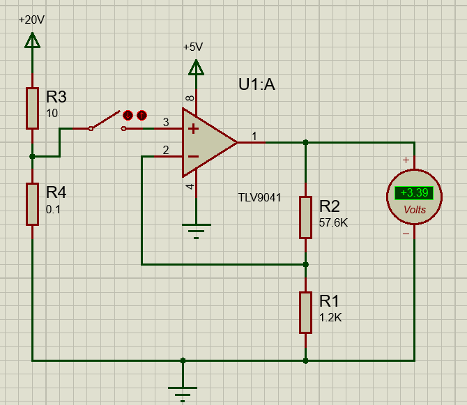
The load current (ILOAD) produces a voltage drop across the shunt resistor (RSHUNT) and is set from 0A to 1A. To keep the shunt voltage below 100mV at maximum load current, the largest shunt resistor is shown; the gain of the circuit can be found by implementing a gain formula.
Applications
- Portable electronics
- Wearable fitness and activity monitor
- Headsets/headphones and earbuds
- Personal electronics
- Building automation
- Wearables (non-medical)
- Motion detector (PIR, uWave, etc.)
- Electronic point of sales (EPOS)
- Single-supply, low-side, unidirectional current sensing circuit
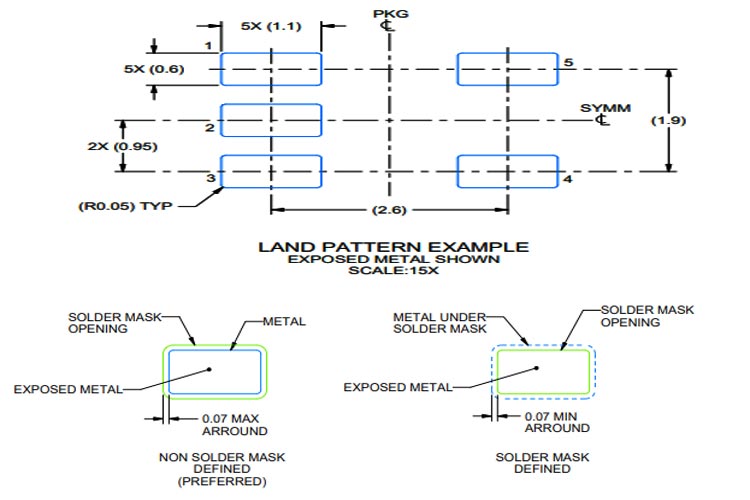
2D Model and Dimensions
If you are designing a PCB or Perf board with this component then the following picture from the Datasheet will be useful to know its package type and dimensions.