LMH6629 High-Speed Op Amp IC
The LMH6629 is a high-speed, ultra-low noise amplifier designed for applications requiring wide bandwidth with high gain and low noise such as in communication, test and measurement, optical and ultrasound systems.
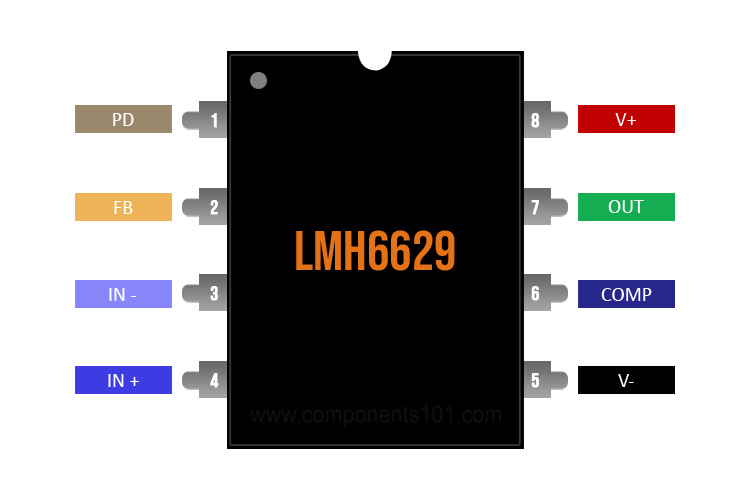
LMH6629 Op-Amp Pinout Configuration
|
Pin Number |
Pin Name |
Description |
|
1 |
PD |
Power Down (Logic Low) |
|
2 |
FB |
Feedback Voltage |
|
3 |
IN- |
Inverting Input |
|
4 |
IN+ |
Non-Inverting Input |
|
5 |
V- |
Negative Supply Voltage |
|
6 |
COMP |
Inverting Input of Op-Amp B |
|
7 |
OUT |
Output of Op-Amp B |
|
8 |
V+ |
Positive Supply Voltage |
Features & Specifications
- Specified for Vs = V. R,100 Ay .10VN WSO" Package. unless Specified. -sea Banc: Width 900 MHz
- Input Voltage Noise 0.69 nV/√Hz
- Input Offset Voltage Max. Over Temperature ±0.8 The LMH6629 operates on 2.7-V to 5.5-V supply with mV
- Slew Rate 1600 V/ μs
- HD2 @ f = 1 MHz, 2VPP −90 dBc
- HD3 @ f = 1 MHz, 2VPP −94 dBc
- Supply Voltage Range 2.7 V to 5.5 V
- Typical Supply Current 15.5 mA
- Selectable Min. Gain ≥4 or ≥10 V/V
- Enable Time: 75 ns
- Output Current ±250 mA
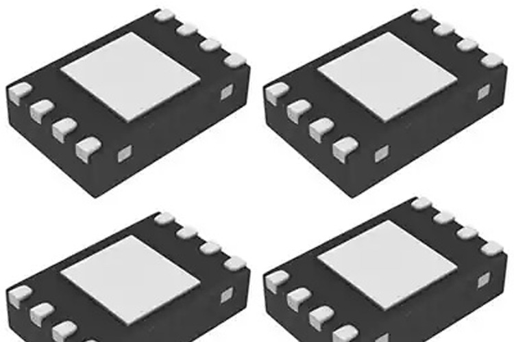
- WSON-8 and SOT-23-5 Packages
Note: Complete Technical Details can be found in the LMH6629 datasheet given at the end of this page.
LMH6629 Equivalent Op-Amp
LM2902, OPA2134, TL074, TL072, TL071
Where to use LMH6629 Op-Amp
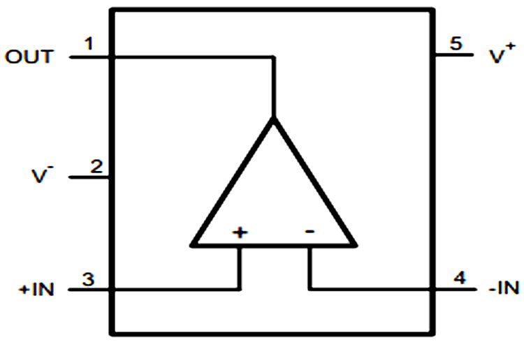
The LMH6629 is a Single Package Operational Amplifier, meaning it has one Op-Amp inside it, this op-amp has many features that we will discuss later.
The LMH6629 operates on a 2.7V to 5.5V supply with an input common-mode range that extends below ground and outputs that swing to within 0.8V of the rails for ease of use in single supply applications. Heavy loads up to ±250mA can be driven by high-frequency large signals with the LMH6629's —3dB bandwidth of 900MHz and 1600V/ps slew rate. The LMH6629 (WSON-8 package only) has user-selectable internal compensation for minimum gains of 4 or 10 controlled by pulling the COMP pin low or high, thereby avoiding the need for external compensation capacitors required in competitive devices.
The low-input noise,(0.69 nV/√Hz and 2.6 pA/√Hz) low distortion (HD2/HD3 = -90 dBc/-94 dBc) and ultra-low DC errors (800 pV Vos maximum over-temperature, ±0.45 pV/°C drift) allow precision operation in both ac- and dc-coupled applications. The LMH6629 is fabricated in Texas Instruments' proprietary SiGe process and is available in a 3mm x 3mm 8-pin WSON package as well as the SOT-23-5 package.
Interesting Features of LMH6629 IC
As this IC falls under the high range category this IC has very interesting parameters that one should eventually look at, if the application in hand is a critical one, in this section we will discuss some of the important technical features.
The LMH6629 WSON-8 package has two digital control pins; PD and COMP pins. The PD pin, used for power down, floats high (device on) when not driven. When the PD pin is pulled low, the amplifier is disabled and the amplifier output stage goes into a high impedance state so the feedback and gain set resistors determine the output impedance of the circuit. The other control pin, the COMP pin, allows control of the internal compensation and defaults to the lower gain mode or logic 0.
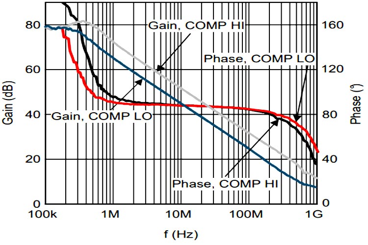
Unless otherwise specified, VS = ±2.5V, Rf = 240 Ω, RL = 100 Ω, VO = 2 VPP, COMP pin = HI, AV = +10 V/V, WSON-8 and SOT-23-5 packages (unless specifically noted)
Open Loop Gain/Phase Response
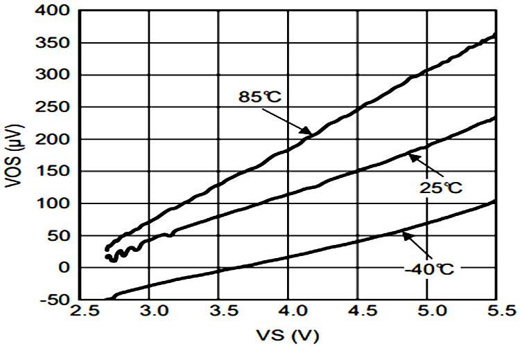
Offset Voltage vs. Supply Voltage
How to use LMH6629 Op-Amp
The LMH6629 is a high gain bandwidth, ultra-low noise voltage feedback operational amplifier. The excellent noise and bandwidth enable applications such as medical diagnostic ultrasound, magnetic tape, and disk storage, and fibreoptics to achieve maximum high-frequency signal-to-noise ratios. The following non-inverting op-amp configuration shows how the device works in certain conditions.
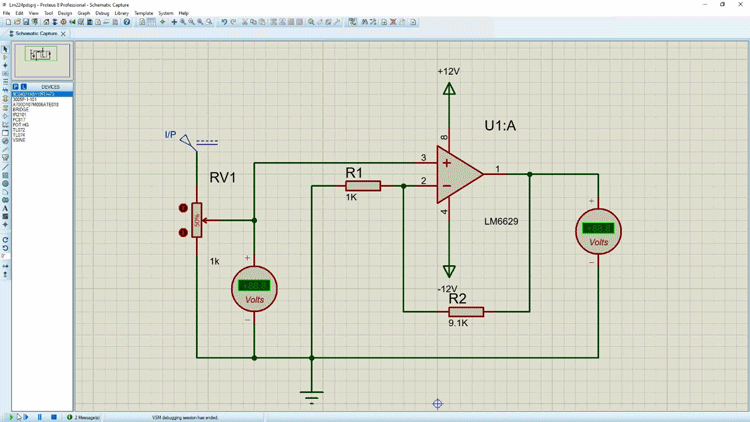
In the above, the LMH6629 Op-amp is configured as a non-inverting configuration. The gain of the op-amp is set to 10. For that we have used a 1K resistor and a 9.1K resistor, as you can see for the simulation we have used a variable potentiometer be varying the potentiometer we can vary the input voltage and the output voltage will also vary, to power the op-amp we have used +12V and -12V supply, as the gain of the op-amp is 10 so if we provide 1V at the input we will get 10V at the output the simulated circuit shows exactly that.
Applications
- Instrumentation Amplifiers
- Ultrasound Preamps
- Wide-band Active Filters
- Opto-Electronics
- Medical Imaging Systems
- Base-Station Amplifiers
- Low-Noise Single-Ended to Differential Conversion
- Trans-Impedance Amplifier
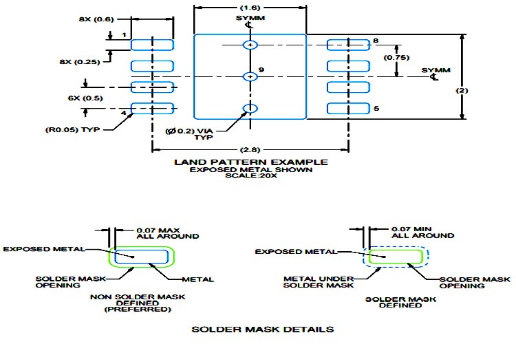
2D Model and Dimensions
If you are designing a PCB or Perf board with this component then the following picture from the Datasheet will be useful to know its package type and dimensions.