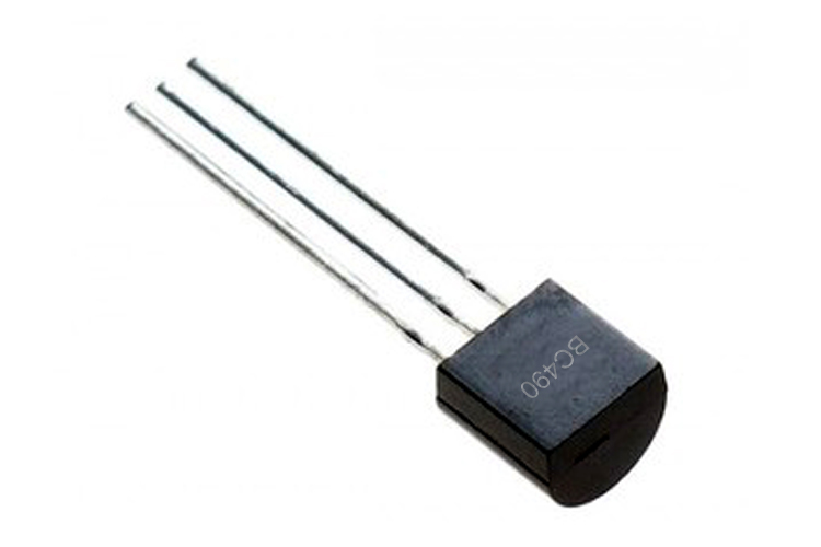
BC490 General Purpose High Current PNP Transistors
The BC490 is a PNP Transistor in a TO-92 package, it has a VCE of -80V and a continuous collector current of -1A DC. With this characteristic and 625mW total power dissipation, this transistor can be used in moderately high voltage switching applications.
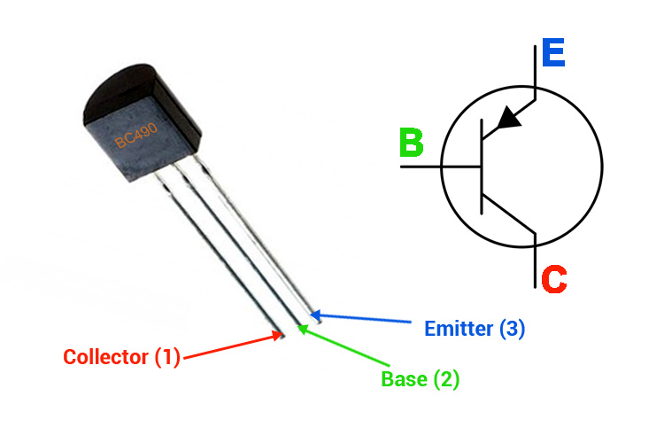
BC490 Transistor Pinout Configuration
|
Pin Number |
Pin Name |
Description |
|
1 |
Collector |
Electrons Emitted from Emitter Collected by the Collector |
|
2 |
Base |
Controls the biasing of the transistor |
|
3 |
Emitter |
Electrons emitted from the emitter into the first PN junction |
Features & Specifications
- Bi-Polar PNP Transistor
- DC Current Gain (hFE) is 400 maximum
- Continuous Collector current (IC) is 1000mA or 1A
- Emitter Base Voltage (VBE) is -4V
- Base Current (IB) is 50mA maximum
- Available in SOT23-3 Package
- Maximum Collector-Base Voltage |Vcb|: -80 V
- Collector Dissipation: 0.625 W
- Transition Frequency:150 MHz
- Operating and Storage Junction Temperature Range -55 to +150 °C
- Collector Capacitance 9 pF
Note: Complete Technical Details can be found in the BC490 transistor datasheet given at the end of this page.
BC490 Equivalent Transistor
Basic Working of a Transistor
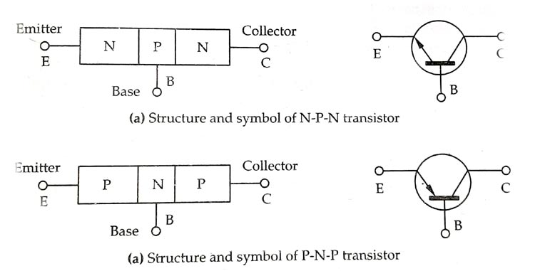
The BC490 Transistor is a general-purpose PNP transistor, A junction transistor is a sandwiched construction between two layers of N-type material or P-type material. Depending upon the construction transistors are divided into two categories NPN transistor and PNP transistor, which are shown below. Transistors are made up of silicon or germanium, depending upon the application it is chosen.
General Description of BC490 Transistor
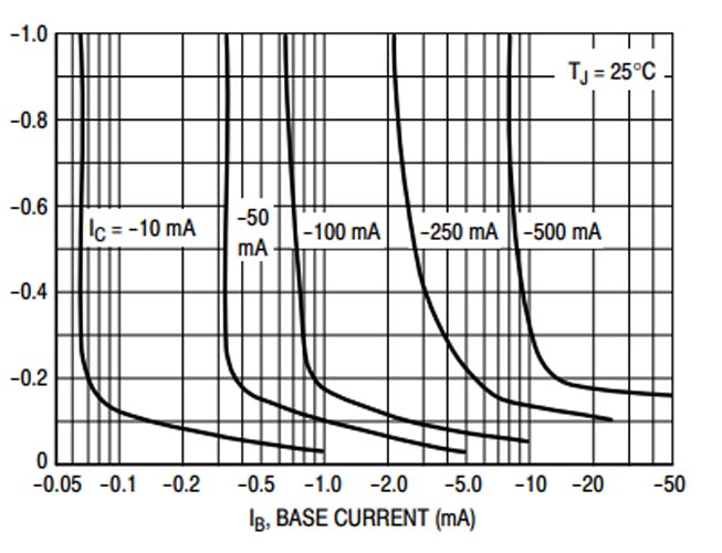
The BC490 can be used in many different applications. This transistor can be used where you want to switch moderately high voltage devices. The component is cheap and easy to work with so it is best suited for switching applications. When this transistor is in a biased condition, then it can allow a maximum current of 1A across CE(Collector-Emitter) Junction, this state of the transistor is called the saturation state, and driving a load that consumes more current than 1A may damage the device permanently, also during the design process, you need to be aware that the maximum dissipation of this device is 625W, power more than that can damage the device. As you already may know a transistor is a current-controlled device so when the base current is removed the transistor becomes fully off, in this stage the transistor is working in its cut-off region/cut-off state and no current flows through the C-E junction. The BC490 Transistor has a gain of 40 to 160, this value determines the amplification capacity of the transistor, the peak current that can be flown through this transistor is 1.5A, which combined with the gain value makes this transistor a perfect choice for moderate-high voltage application.
Under normal circumstances and without external influence there will be a positive voltage appearing at the base of the PNP transistor. As we all know, based on the working principle of a PNP transistor; having a positive voltage at the base puts a PNP transistor in a high resistance state. By characteristic a small amount of current needs to flow out of the base of the transistor to completely turn on the device, for this device you can see, in order to flow 1000mA of current through the collector to emitter, 50mA of current needed to flow through the base of the transistor.
How to use BC490 Transistor
Transistors are current-controlled devices so to turn them on a little current is needed. For the BC490 Transistor, this base current is less than 50mA, as BC490 is a PNP transistor that means it will be on when the base is connected to the ground, and it will be off when a positive voltage is applied to the base of the transistor.
The simulated circuit below shows how this transistor behaves when the base of the basic circuit is connected to the ground and when it's connected to 5V of the power supply.
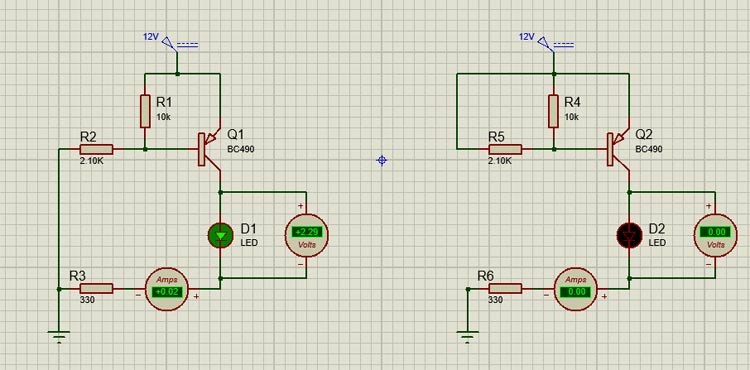
When we turn on the transistor by connecting the base to the supply the transistor will remain on unless the voltage at the base of the transistor reaches less than the cut-off voltage of the transistor that is 0.7-0.9V. The base of the transistor cannot be left floating otherwise there could be false triggering, which may lead to issues in the circuit, to resolve the issue we need to add pulldown resistors as shown in the example a 10K resistor is used to pull up the base of the transistor to VCC.
Applications
- Simple switching applications
- Microphone preamplifiers
- Lighting systems
- Relay drivers
- Audio Amplifiers
- Signal Amplifiers
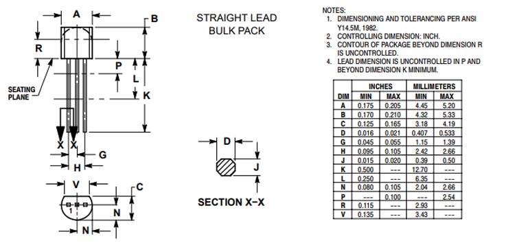
2D Model and Dimensions
If you are designing a PCB or Perf board with this component then the following picture from the Datasheet will be useful to know its package type and dimensions.